Board thermal coupling
Where does the heat go? A powered board is a heat-conduction problem, and PcbThermal solves it
on the landed FEA thermal solver — not a lumped estimate — so its answers
are verifiable against closed forms. Each component’s dissipation becomes a volumetric heat source
in the board; the copper spreads it sideways; a cold edge or a convecting face carries it away; and
the result is a temperature field the viewer’s colour map picks up with no extra
wiring, plus a hot-spot temperature per component.
The model: an effective conductivity over a slab
A board is a copper–dielectric sandwich, and v1 uses the standard board-level model: the copper is not meshed as discrete traces and planes, it is smeared into an effective conductivity over a homogeneous slab. The mixing rule is the physics of the sandwich:
- In-plane the copper layers are PARALLEL heat paths, so the effective conductivity is the
area-fraction rule of mixtures,
k_in = f·k_Cu + (1 − f)·k_FR4. - Through-thickness the layers are in SERIES, so it is the harmonic mean,
k_th = 1 / (f/k_Cu + (1 − f)/k_FR4).
f is the copper VOLUME fraction — (total copper thickness × average coverage) / board thickness —
the one honest knob. A bare board (f = 0) collapses both to the dielectric’s own conductivity (an
isotropic slab). This is the standard model because it needs no conforming multi-material mesh; a
future stage can refine it by meshing the copper explicitly.
A powered board
A small board with a hot regulator and a warm microcontroller, edge-clamped to a chassis and cooling through its faces:
var mcu = new PartDefinition("MCU", "U", new[] { new Pin("1", PinType.Passive) },    new Footprint("qfp", new[] { new Pad("1", new Vector2d(0, 0), 7, 7, PadShape.Rectangular) }));var reg = new PartDefinition("REG", "U", new[] { new Pin("1", PinType.Passive) },    new Footprint("sot", new[] { new Pad("1", new Vector2d(0, 0), 4, 4, PadShape.Rectangular) }));
var sch = new Schematic("gadget");sch.Add("U1", mcu);sch.Add("U2", reg);
var board = new PcbBoard(    new[] { new Vector2d(0, 0), new Vector2d(50, 0), new Vector2d(50, 30), new Vector2d(0, 30) },    thickness: 1.6);var layout = new PcbLayout(sch, board);layout.Place("U1", 15, 15);   // the MCU, mid-boardlayout.Place("U2", 40, 15);   // the regulator, out near the far edge
var spec = new PcbThermalSpec{    // A modest ground-plane fraction: two 35 um layers at ~55% average coverage.    CopperFraction = 2 * 0.035 * 0.55 / 1.6,    ComponentPower = new Dictionary<string, double> { ["U1"] = 0.4, ["U2"] = 1.2 },   // watts    Boundaries = new[]    {        // The −X edge clamps to a 40 C chassis rail; the faces convect to 40 C air.        PcbThermalBoundary.FixedTemperature("chassis",            Facets.OnPlane(new Vector3d(0, 0, 0), Vector3d.UnitX), 40),        PcbThermalBoundary.Convection(BoardSurface.Top, 15, 40),        PcbThermalBoundary.Convection(BoardSurface.Bottom, 15, 40),    },};
var result = PcbThermal.Solve(layout, spec);Console.WriteLine(result);   // temperature range, effective conductivities, applied wattsforeach (var (reference, temp) in result.ComponentTemperature)    Console.WriteLine($"  {reference} hot-spot: {temp:g5} C");
// The regulator dissipates 3x the MCU and sits further from the cold rail, so it runs hotter.if (result.TemperatureOf("U2") <= result.TemperatureOf("U1"))    throw new Exception("the regulator should be the hot spot");
result is a PcbThermalResult: the board’s PeakTemperature / MinTemperature, a
ComponentTemperature map (each component’s hot-spot — the peak under its footprint), the effective
ConductivityInPlane / ConductivityThrough, and the underlying FEA ThermalResults.Fea (heat
flux, .vtu export, the solve report). Power is stated in watts — the domain’s universal unit —
and converted once to the model’s milliwatt; a convection film coefficient is stated in
W/(m²·K) (natural air ~10, a fan ~50).
Seeing it
The board coloured by temperature, the two sources standing on it:
var mcu = new PartDefinition("MCU", "U", new[] { new Pin("1", PinType.Passive) },    new Footprint("qfp", new[] { new Pad("1", new Vector2d(0, 0), 7, 7, PadShape.Rectangular) }),    body: () => Shape.Box(9, 9, 1.4).Translate(0, 0, 0.7));var reg = new PartDefinition("REG", "U", new[] { new Pin("1", PinType.Passive) },    new Footprint("sot", new[] { new Pad("1", new Vector2d(0, 0), 4, 4, PadShape.Rectangular) }),    body: () => Shape.Box(6, 5, 1.6).Translate(0, 0, 0.8));
var sch = new Schematic("gadget");sch.Add("U1", mcu);sch.Add("U2", reg);
var board = new PcbBoard(    new[] { new Vector2d(0, 0), new Vector2d(50, 0), new Vector2d(50, 30), new Vector2d(0, 30) },    thickness: 1.6);var layout = new PcbLayout(sch, board);layout.Place("U1", 15, 15);layout.Place("U2", 40, 15);
var spec = new PcbThermalSpec{    CopperFraction = 2 * 0.035 * 0.55 / 1.6,    ComponentPower = new Dictionary<string, double> { ["U1"] = 0.4, ["U2"] = 1.2 },    Boundaries = new[]    {        PcbThermalBoundary.FixedTemperature("chassis",            Facets.OnPlane(new Vector3d(0, 0, 0), Vector3d.UnitX), 40),        PcbThermalBoundary.Convection(BoardSurface.Top, 15, 40),        PcbThermalBoundary.Convection(BoardSurface.Bottom, 15, 40),    },};var result = PcbThermal.Solve(layout, spec);
// The board part, coloured by the sampled temperature field.var boardPart = new Part("board", board.Plate());foreach (var field in result.SampleOnto(boardPart.GetMesh()))    boardPart.AddResult(field);boardPart.FieldDisplay = new FieldDisplay { Field = ThermalResults.FieldNames.Temperature };
var assembly = new Assembly("thermal");assembly.Add(boardPart, layout.BoardFrame, "board");foreach (var placement in layout.Placements){    var definition = layout.Schematic.Find(placement.Reference).Definition;    if (definition.Body is null) continue;    var part = new Part(placement.Reference, definition.Body())    {        Transform = PcbLayout.PartTransform(placement.Side),    };    assembly.Add(part, layout.OccurrenceFrame(placement), placement.Reference);}
var scene = new Scene();scene.AddTab("Thermal").Add(assembly);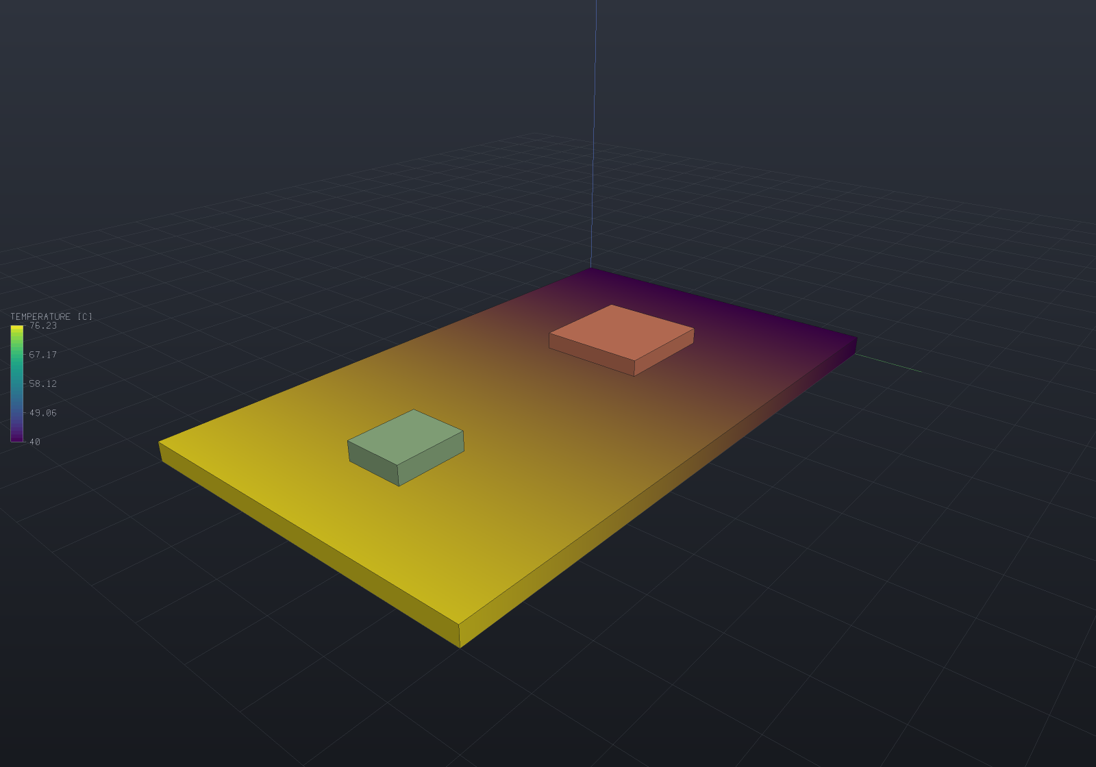
The dark band is the clamped 40 °C edge; the board warms toward the regulator, whose footprint is the peak. The copper plane smears the two sources into one smooth field.
Verified against closed forms
An ECAD thermal answer fails plausibly, so the module is held against analytic conduction rather than against a picture (the FEA house style):
- A uniformly-dissipating board to a fixed cold edge settles into the parabola
T(x) = T0 + (q/2k)(L² − x²)— which lives in the quadratic element space, so the solve reproduces it to 3e-12 relative (round-off). The stated watts come out as exactlyP × 1000mW of applied heat (the units check). - A single hot component past a cold edge carries all its power as a constant flux, so the
far-field profile is the series-resistance line
T = T0 + Q(L − x)/(kA), matched to 3.6e-5 (the 3D discretization of a localized source), with the energy balance — all the generated heat leaves the cold edge — exact to round-off. - Copper raises spreading. The same 0.3 W source over real FR4 (k = 0.3) versus FR4 with 2.6 %
copper lifts the effective in-plane conductivity from 0.3 to 10.4 and drops the peak rise
1129 K → 32.6 K (34.7× lower); the far-field rise ratio is exactly
k_copper / k_bare. - A board with no boundary condition is an undriven conduction problem, refused by name (the
ThermalSolverconvention); a zero-power board is isothermal at its held temperature exactly; and a solve is deterministic to the bit.
Not in v1
Filed as later stages, each with its own oracle:
- Transient board warm-up — the
SolveTransientpath exists, so it is a bounded follow-on with its own erfc-style oracle; the effective slab already carries a volume-weighted heat capacity. - Thermal vias as discrete high-conductivity paths — v1’s effective conductivity smears the copper, so it smears the vias too.
- Airflow / CFD convection — v1 takes a stated film coefficient, not a flow field.
- Detailed die/package thermal models — v1 spreads a component’s power uniformly over its footprint volume, not through a junction-to-case network.