Loading a component (symbol + footprint)
A PartDefinition in EngrCAD is built from the three views of one part: its 2D
schematic symbol (the drawn shape a schematic sheet wires to), its footprint (the copper
pads the board places), and its 3D model (the body an assembly seats) — all sharing one
pin-NUMBER identity, plus the pins that are the netlist terminals. Stage 1 could declare pins
and a footprint by hand; a real library is imported, so EngrCAD reads a component from the
KiCad interchange (.kicad_sym + .kicad_mod) or an Eagle library (.lbr) so it
arrives with all three at once.
The one identity: one part, one set of pin NUMBERS
The three representations are one identity by pin number: symbol pin "1" == footprint pad
"1" == netlist pin "1". That is the whole point of loading symbol and footprint together —
and a PinIdentity check verifies it, naming any symbol pin with no pad, pad with no pin, or
pin with neither. It is the one-declaration rule (the schematic’s source of truth) extended to
the drawn symbol.
Loading a resistor
ComponentLibrary.Read (text) / ComponentLibrary.Load (files) reads the symbol and the
footprint and unifies them:
// A minimal KiCad symbol library (.kicad_sym) — one resistor, two passive pins, a body.var symText = """(kicad_symbol_lib (version 20211014) (generator kicad_symbol_editor)  (symbol "R_0805"    (property "Reference" "R" (at 2.032 0 90) (effects (font (size 1.27 1.27))))    (property "Value" "R_0805" (at 0 0 90) (effects (font (size 1.27 1.27))))    (property "Footprint" "Resistor_SMD:R_0805_2012Metric" (at 0 0 0)      (effects (font (size 1.27 1.27)) hide))    (symbol "R_0805_0_1"      (rectangle (start -1.016 2.54) (end 1.016 -2.54)        (stroke (width 0.254) (type default)) (fill (type none))))    (symbol "R_0805_1_1"      (pin passive line (at 0 3.81 270) (length 1.27)        (name "~" (effects (font (size 1.27 1.27))))        (number "1" (effects (font (size 1.27 1.27)))))      (pin passive line (at 0 -3.81 90) (length 1.27)        (name "~" (effects (font (size 1.27 1.27))))        (number "2" (effects (font (size 1.27 1.27))))))))""";
// The matching KiCad footprint (.kicad_mod) — two SMD pads, in millimetres.var modText = """(footprint "R_0805_2012Metric" (version 20211014) (generator pcbnew) (layer "F.Cu") (attr smd)  (pad "1" smd roundrect (at -0.9125 0) (size 1.025 1.4)    (layers "F.Cu" "F.Paste" "F.Mask") (roundrect_rratio 0.243902))  (pad "2" smd roundrect (at 0.9125 0) (size 1.025 1.4)    (layers "F.Cu" "F.Paste" "F.Mask") (roundrect_rratio 0.243902)))""";
var part = ComponentLibrary.Read(symText, modText);var def = part.Definition;
// It arrives with pins, a footprint AND a symbol — one part, one set of pin numbers.Console.WriteLine($"{def.Name}: {def.Pins.Count} pins, "    + $"{def.Footprint!.Pads.Count} pads, {def.Symbol!.Pins.Count} symbol pins");
if (def.Pins.Count != 2) throw new Exception("expected two pins");if (def.ReferencePrefix != "R") throw new Exception("expected reference prefix R");
// The identity holds: symbol pin "1" == pad "1" == netlist pin "1".if (!part.Identity.Ok) throw new Exception(part.Identity.ToString());
// A symbol pin's ANCHOR is where a wire lands. Pin 1 sits above the body, pointing down.var pin1 = def.Symbol.PinNumbered("1");Console.WriteLine($"pin 1 anchor {pin1.Anchor}, points {pin1.Direction}, "    + $"meets body at {pin1.Inner}");
// The pad coordinates are STATED in the file, so they are carried exactly.if (def.Footprint.Pads[0].Center.X != -0.9125) throw new Exception("pad geometry drifted");
// A loaded part is data now: it round-trips through the schematic file byte-for-byte.var sch = new Schematic("one resistor");sch.Add("R1", def, value: "330");var json = sch.Save();if (Schematic.Load(json).Save() != json)    throw new Exception("the loaded symbol is not a persistence fixed point");
The symbol is the representation a drawn schematic sheet consumes — each SymbolPin carries
the point where a wire lands (Anchor), the direction it points into the body, and its length,
so routing a wire to a placed symbol is exact.
Loading from Eagle (.lbr)
An Eagle library is a single XML file (.lbr), read with EagleLibraryReader — the second
interchange, producing the same LoadedPart. Its structure is different: an Eagle symbol’s pins
are named in the symbol’s own vocabulary, a package’s pads are numbered, and a deviceset’s
<connect gate pin pad> map binds them — so the <connect> map is what unifies the three by pad
number (symbol pin "VCC" → pad "8", so the loaded pin is numbered "8" and named "VCC").
Read the library, then load one device by its full name (deviceset + device):
// A minimal Eagle .lbr library — a resistor deviceset binding a symbol to an 0805 package// through its <connect> map. Eagle stores coordinates in millimetres.var lbr = """<?xml version="1.0" encoding="utf-8"?><eagle version="7.7.0">  <drawing>    <library>      <packages>        <package name="R0805">          <smd name="1" x="-0.9125" y="0" dx="1.025" dy="1.4" layer="1" roundness="25"/>          <smd name="2" x="0.9125" y="0" dx="1.025" dy="1.4" layer="1" roundness="25"/>        </package>      </packages>      <symbols>        <symbol name="R">          <rectangle x1="-1.016" y1="-2.54" x2="1.016" y2="2.54" layer="94"/>          <pin name="1" x="0" y="3.81" length="short" direction="pas" rot="R270"/>          <pin name="2" x="0" y="-3.81" length="short" direction="pas" rot="R90"/>        </symbol>      </symbols>      <devicesets>        <deviceset name="R-EU_" prefix="R">          <gates><gate name="G$1" symbol="R" x="0" y="0"/></gates>          <devices>            <device name="R0805" package="R0805">              <connects>                <connect gate="G$1" pin="1" pad="1"/>                <connect gate="G$1" pin="2" pad="2"/>              </connects>            </device>          </devices>        </deviceset>      </devicesets>    </library>  </drawing></eagle>""";
// Read the library, then load one device by its full name (deviceset + device).var lib = EagleLibraryReader.Read(lbr);Console.WriteLine("devices: " + string.Join(", ", lib.Devices.Select(d => d.Name)));
var part = lib.Load("R-EU_R0805");var def = part.Definition;Console.WriteLine($"{def.Name}: {def.Pins.Count} pins, {def.Footprint!.Pads.Count} pads, "    + $"{def.Symbol!.Pins.Count} symbol pins");
// The <connect> map unifies the three: symbol pin "1" == pad "1" == netlist pin "1".if (!part.Identity.Ok) throw new Exception(part.Identity.ToString());if (def.ReferencePrefix != "R") throw new Exception("expected reference prefix R");
// Pad coordinates are STATED in the file (millimetres), so they are carried exactly.if (def.Footprint.Pads[0].Center.X != -0.9125) throw new Exception("pad geometry drifted");
// A symbol pin's ANCHOR is where a wire lands; rot=R270 points the pin down.var pin1 = def.Symbol.PinNumbered("1");Console.WriteLine($"pin 1 anchor {pin1.Anchor}, points {pin1.Direction}");if (pin1.Direction != SymbolPinDirection.Down) throw new Exception("pin direction drifted");
// The loaded part is data: it round-trips through the schematic file byte-for-byte.var sch = new Schematic("one resistor");sch.Add("R1", def, value: "330");var json = sch.Save();if (Schematic.Load(json).Save() != json) throw new Exception("not a persistence fixed point");
Eagle’s covered subset mirrors KiCad’s: symbol wire/rectangle/circle/polygon/text
graphics and pins (a pin’s rot gives its direction, length its length, direction its
PinType), and package smd pads and pad plated through-holes of the standard shapes
(round/square/octagon/long) with their drill. A package <hole>/<via> (not a pad), a graphic
kind outside the set, a multi-gate deviceset (a gate array), and a symbol pin with no <connect>
(an unmapped pin) are each ignored with a diagnostic or refused by name; a .brd/.sch handed
to the library reader is refused at the root, signposted to EagleSchematicReader /
EagleBoardReader (both below) — a user holding any Eagle file is pointed at the right door.
Loading a whole Eagle schematic (.sch)
EagleSchematicReader.Read imports a whole Eagle schematic, and it is the structural opposite of
the KiCad one below: where a .kicad_sch only draws its netlist (connectivity reconstructed from
wire geometry), an Eagle schematic declares it — every <net> lists its
<pinref part gate pin> terminals — so the import is a resolution, not a reconstruction, and the
wire geometry is never consulted. Parts resolve through the schematic’s own embedded <libraries>
(each the same content as a .lbr’s, read by the shared library machinery, definitions interned per
device); a part whose device cannot be assembled — typically a supply symbol, whose deviceset has
no connects — is reported and skipped, its nets surviving because an Eagle net carries its own name.
A pinref names the symbol pin, resolved by name first (so pin="VCC" lands on pad 8, which a
number-blind resolver cannot do); nets group by name across every sheet (Eagle nets are global to the
schematic), a one-pin net becomes a stub, and unloadable parts / unknown pinrefs are reported, never
thrown.
Loading a whole Eagle board (.brd)
EagleBoardReader.Read is the board twin. A .brd’s <signal>s declare their terminals too
(<contactref element pad>), so the synthesized schematic is the file’s own intent — and that is
what makes the import checkable rather than hopeful: the imported copper (layer-1/16 wires as
traces, <via>s as through-vias) must actually join the declared pads, which Connectivity()
confirms. Elements reference packages directly (no deviceset in a board), resolved through the
embedded <libraries> by the same shared machinery; the outline is the chained layer-20 <plain>
wires; a rotation MR… is mirrored, landing the element on the bottom side; an absent via
diameter takes Eagle’s own auto-restring rule (pad = drill + 2·max(25% drill, 0.254 mm), a
transcribed nominal). A signal <polygon> becomes a copper pour — isolate is the clearance,
orphans="on" keeps dead copper, thermals="off" direct-connects pads, and Eagle’s rank (1 =
highest priority) maps to Priority = 6 − rank — so a GND plane joins its pads through the
imported pour alone. Airwires (layer 19 — the ratsnest, intent not copper), inner-layer wires
and curved wires are reported and skipped or flattened by name — the covered
copper subset is the two-layer board — and the thickness is assumed 1.6 mm with a note, since a
.brd does not state it.
// A minimal Eagle board: two 0805 resistors (one rotated 90°) on a 30×20 outline, one declared// signal, and the top-layer wire that routes it. The import resolves the packages, chains the// outline, places the parts and carries the copper — then the connectivity CHECK proves the// routed wire really joins the declared pads (a wrong placement transform would break it).var brdText = """<?xml version="1.0"?><eagle version="7.7.0">  <drawing>    <board>      <libraries>        <library name="passives">          <packages>            <package name="R0805">              <smd name="1" x="-0.9125" y="0" dx="1.025" dy="1.4" layer="1"/>              <smd name="2" x="0.9125" y="0" dx="1.025" dy="1.4" layer="1"/>            </package>          </packages>        </library>      </libraries>      <plain>        <wire x1="0" y1="0" x2="30" y2="0" width="0.1" layer="20"/>        <wire x1="30" y1="0" x2="30" y2="20" width="0.1" layer="20"/>        <wire x1="30" y1="20" x2="0" y2="20" width="0.1" layer="20"/>        <wire x1="0" y1="20" x2="0" y2="0" width="0.1" layer="20"/>      </plain>      <elements>        <element name="R1" library="passives" package="R0805" x="8" y="10"/>        <element name="R2" library="passives" package="R0805" x="22" y="10" rot="R90"/>      </elements>      <signals>        <signal name="SIG">          <contactref element="R1" pad="2"/>          <contactref element="R2" pad="1"/>          <wire x1="8.9125" y1="10" x2="22" y2="9.0875" width="0.3" layer="1"/>        </signal>      </signals>    </board>  </drawing></eagle>""";
var board = EagleBoardReader.Read(brdText);var layout = board.Layout;Console.WriteLine($"{layout.Placements.Count} placements, {layout.Traces.Count} trace, "    + $"{layout.Schematic.Nets.Count} net");// R2 is rotated 90°: its pad 1 lands at (22, 9.0875) — the file's own millimetres, exactly.var r2Pad1 = layout.PlacedPads().Single(p => p.Name == "R2.1");Console.WriteLine($"R2.1 at ({r2Pad1.World.X}, {r2Pad1.World.Y})");Console.WriteLine($"SIG joined by the imported copper: {layout.Connectivity().Of("SIG").IsConnected}");
Managed Eagle libraries and their 3D packages (<packages3d>)
Eagle 9 (and Fusion) keeps libraries managed: every library, package, symbol and deviceset
carries a urn, and a new <packages3d> block declares 3D packages that devices bind through
<package3dinstances>. The additive urn/library_version attributes need no handling at all —
a reader that asks for its attributes by name never sees them — so the classic subset (pads,
pins, the <connect> map) reads exactly as it does from a pre-9 .lbr.
The <packages3d> binding is the real difference, and it comes with one honest problem: a
managed library states an identity, not a path. A <package3d> is a name plus a URN plus the 2D
packages its <packageinstance>s bind; the model file lives in Fusion’s cloud, keyed by that
URN, and the .lbr does not carry it. So the reader surfaces the binding as data and attaches
a ComponentModel3D only when a resolver you supply finds a local file that exists — never
guessing a path into geometry:
// A managed (Eagle 9) library: the classic content plus urn attributes and a <packages3d> block.var lbr = """<?xml version="1.0" encoding="utf-8"?><eagle version="9.6.2">  <drawing>    <library urn="urn:adsk.eagle:library:325">      <packages>        <package name="R0805" urn="urn:adsk.eagle:footprint:23122/1" library_version="1">          <smd name="1" x="-0.9125" y="0" dx="1.025" dy="1.4" layer="1" roundness="25"/>          <smd name="2" x="0.9125" y="0" dx="1.025" dy="1.4" layer="1" roundness="25"/>        </package>      </packages>      <packages3d>        <package3d name="RESC2012X70N" urn="urn:adsk.eagle:package:23123/2" type="model" library_version="1">          <packageinstances><packageinstance name="R0805"/></packageinstances>        </package3d>      </packages3d>      <symbols>        <symbol name="R" urn="urn:adsk.eagle:symbol:16966/1">          <rectangle x1="-1.016" y1="-2.54" x2="1.016" y2="2.54" layer="94"/>          <pin name="1" x="0" y="3.81" length="short" direction="pas" rot="R270"/>          <pin name="2" x="0" y="-3.81" length="short" direction="pas" rot="R90"/>        </symbol>      </symbols>      <devicesets>        <deviceset name="R-EU_" prefix="R" urn="urn:adsk.eagle:component:23134/1">          <gates><gate name="G$1" symbol="R" x="0" y="0"/></gates>          <devices>            <device name="R0805" package="R0805">              <connects>                <connect gate="G$1" pin="1" pad="1"/>                <connect gate="G$1" pin="2" pad="2"/>              </connects>              <package3dinstances>                <package3dinstance package3d_urn="urn:adsk.eagle:package:23123/2"/>              </package3dinstances>            </device>          </devices>        </deviceset>      </devicesets>    </library>  </drawing></eagle>""";
var lib = EagleLibraryReader.Read(lbr);
// The 3D packages are DATA: a name, the URN that identifies the model, its type, and the 2D// packages it binds.foreach (var p3d in lib.Packages3d)    Console.WriteLine($"{p3d.Name} [{p3d.Type}] {p3d.Urn} -> {string.Join(", ", p3d.PackageNames)}");if (lib.Packages3d.Count != 1) throw new Exception("expected one 3D package");
// A device names the URN it binds, so a caller can resolve it however it likes.var device = lib.Devices.Single(d => d.Name == "R-EU_R0805");Console.WriteLine($"{device.Name} binds {device.Package3dUrn}");
// With no resolver, the binding is RECORDED by name and no model is attached — the geometry is// cloud content this file does not carry, so inventing one would be a lie.var plain = lib.Load("R-EU_R0805");if (plain.Definition.Model is not null) throw new Exception("nothing should have been attached");Console.WriteLine(plain.Diagnostics.First(d => d.Contains("23123/2")));
// A resolver is asked about the bound 3D package and answers with a LOCAL path, or null. Here it// has no local copy, so the binding is still only recorded — and it says so.string? asked = null;var resolved = lib.Load("R-EU_R0805", p3d => { asked = p3d.Urn; return null; });Console.WriteLine($"the resolver was asked about {asked}");if (resolved.Definition.Model is not null) throw new Exception("no local copy: nothing to attach");
// The classic three representations are untouched by any of this.if (!resolved.Identity.Ok) throw new Exception(resolved.Identity.ToString());if (resolved.Definition.Footprint!.Pads[0].Center.X != -0.9125) throw new Exception("pad drifted");
Return a real path from the resolver — a .stl/.obj/.off/.wrl/.step file you have
downloaded or keep beside the library — and the definition arrives with an ordinary
ComponentModel3D at the identity placement (an Eagle <package3d> states no offset; Fusion
aligns the model to the footprint origin), which then seats, exports and round-trips exactly like a
KiCad-referenced model.
Everything the reader cannot verify is reported by name rather than assumed: no resolver, a
resolver with no local copy, a resolver naming a file that is not there, a device binding a URN the
library never declares, a <package3d> whose <packageinstance> names a package the library
lacks, and a device binding a second 3D package (a PartDefinition carries one model, so the
first wins and the rest are named). A <package3d> with no urn is dropped by name — the URN
is its identity, since that is what a device’s binding references. A file declaring version 9 or
newer also gets a diagnostic naming the version, in all three Eagle readers, so managed provenance
is visible rather than silent; a classic file gets none. Fetching a URN’s model from the cloud is
deliberately not done: it would make an import non-deterministic and unavailable offline, and
the URN is exactly the key you need to do it yourself.
Loading a whole schematic (.kicad_sch)
Loading a component gives one part; loading a .kicad_sch gives a whole schematic — the
connectivity. The board twin (.kicad_pcb) already exists; KiCadSchReader.Read is the schematic
member of the KiCad set. The crux is that a schematic never lists its netlist — it draws it, so
the connectivity is IMPLICIT in the geometry. The reader reconstructs it with a union-find over the
connection points, the same “two things are one net iff they touch” rule the copper connectivity
uses: a wire joins its two endpoints; a pin, a label, a power-symbol pin or a junction lying on a wire
joins it (a junction at a crossing joins both crossing wires); two points carrying the same label are
one net; a no_connect marks a pin unconnected. Two wires crossing with no junction stay two nets:
// A minimal KiCad schematic (.kicad_sch): a two-resistor divider between VCC and GND, with the// mid-point wire named by a local label. Nothing in the file lists the netlist — the reader works// out which pins share a net from the WIRE GEOMETRY (a placed Device:R at (x, y, 0) puts pin "1" at// (x, y - 3.81) and pin "2" at (x, y + 3.81), so a wire endpoint there connects that pin).var schText = """(kicad_sch (version 20230121) (generator eeschema) (paper "A4") (title_block (title "divider"))  (lib_symbols    (symbol "Device:R" (property "Reference" "R" (at 2.032 0 90)) (property "Value" "R" (at 0 0 90))      (symbol "R_1_1"        (pin passive line (at 0 3.81 270) (length 1.27) (name "~") (number "1"))        (pin passive line (at 0 -3.81 90) (length 1.27) (name "~") (number "2"))))    (symbol "power:VCC" (power) (property "Reference" "#PWR" (at 0 0 0)) (property "Value" "VCC" (at 0 3.556 0))      (symbol "VCC_1_1" (pin power_in line (at 0 0 90) (length 0) (name "VCC") (number "1"))))    (symbol "power:GND" (power) (property "Reference" "#PWR" (at 0 0 0)) (property "Value" "GND" (at 0 -3.81 0))      (symbol "GND_1_1" (pin power_in line (at 0 0 270) (length 0) (name "GND") (number "1")))))
  (symbol (lib_id "Device:R") (at 50 40 0) (property "Reference" "R1" (at 53 40 0)) (property "Value" "10k" (at 53 42 0)))  (symbol (lib_id "Device:R") (at 50 60 0) (property "Reference" "R2" (at 53 60 0)) (property "Value" "20k" (at 53 62 0)))  (symbol (lib_id "power:VCC") (at 50 30 0) (property "Reference" "#PWR01" (at 50 27 0)) (property "Value" "VCC" (at 50 26 0)))  (symbol (lib_id "power:GND") (at 50 70 0) (property "Reference" "#PWR02" (at 50 74 0)) (property "Value" "GND" (at 50 75 0)))
  (wire (pts (xy 50 30) (xy 50 36.19)))  (wire (pts (xy 50 43.81) (xy 50 56.19)))  (wire (pts (xy 50 63.81) (xy 50 70)))  (label "MID" (at 50 50 0) (effects (font (size 1.27 1.27))))  (sheet_instances (path "/" (page "1"))))""";
var read = KiCadSchReader.Read(schText);var sch = read.Schematic;
// Power symbols name nets, they are not components — so three symbols place two components.Console.WriteLine($"{sch.Name}: {sch.Components.Count} components, {sch.Nets.Count} nets");Console.WriteLine(sch.ToNetlist().ToText());
// The MID label names the wire joining R1.2 and R2.1 — reconstructed from the geometry.var netlist = sch.ToNetlist();var mid = netlist.NetOf(sch.Find("R1")!.Pin("2"));if (mid?.Name != "MID") throw new Exception("MID net not reconstructed");if (!ReferenceEquals(mid, netlist.NetOf(sch.Find("R2")!.Pin("1"))))    throw new Exception("R1.2 and R2.1 should share the MID net");
// Every component's pins come from its lib_symbol, so the symbol == netlist identity holds by number.foreach (var component in sch.Components)    if (!PinIdentity.Check(component.Definition).Ok) throw new Exception("pin identity");
// The counting identity holds — every pin is on exactly one net.if (!sch.Check().Ok) throw new Exception(sch.Check().ToString());
KiCadSchReader.Read covers a single sheet: the embedded lib_symbols (mapped to
PartDefinitions), placed (symbol …) instances, power symbols (their Value is the net name),
wire, junction, local label, global_label, no_connect, and buses (see below). Refused
by name: a NESTED bus group ({A {B C}}) and a malformed bus range (DATA[], a
non-integer bound); and — in the single-sheet Read only — hierarchical sheets (sheet
subsheets, hierarchical_label), so a flat import cannot silently drop a whole subsheet. A netless
wire, an instance referencing an unknown symbol, a dangling pin, or a dangling / non-member bus entry
is reported as a diagnostic, not thrown; a non-(kicad_sch …) root — a board or a symbol library
handed here — or a malformed S-expression is refused by name.
Buses
A bus is a labelled bundle of signal nets: DATA[0..7] is the eight nets DATA0..DATA7 (KiCad’s
bus-vector notation). A (bus …) wire carries the bundle, a (bus_entry …) rips a member off it onto
a signal wire, and — this is KiCad’s rule — that ripped wire is labelled with the member’s own name
(DATA3), so the member’s net is reconstructed like any other labelled wire. The honest finding is
that a ripped tap’s net is its own local label, and same-named labels are already one net by
local-label equivalence, so on a flat sheet the bus’s connecting role is subsumed. Buses are
therefore sugar: the reader expands a bus label into its members (so a bus label is
NOT mistaken for a signal net — DATA[0..7] is never a net) and validates that each tap is a declared
member, reporting a stray tap by name. All three KiCad bus forms are handled — a vector
NAME[m..n] (a reversed range DATA[7..0] is legal, the same members), an anonymous group
{SDA SCL DATA[0..1]} (its whitespace-separated tokens, each a bare signal or a vector expanded in
turn), and a named alias (a (bus_alias "PCI" (members …)) definition, a bare label matching an
alias read as that bus). Across sheets the connecting role is load-bearing, and it is supported:
a bus sheet pin (a sheet pin whose name is a bus) matched with the sub-sheet’s hierarchical bus
label of the same name carries each member over the boundary — for each member M, the parent’s local
net named M joins the child’s — so a DATA[0..1] bundle into a subsheet gives DATA0 and DATA1 each
spanning the boundary while staying two distinct nets. A nested group ({A {B C}}) is refused by name.
// A DATA[0..1] bus. The DATA[0..1] label declares the members DATA0, DATA1; each bus_entry rips a// member off the bus onto a signal wire that carries the member's OWN label. DATA0 is ripped TWICE// (at R0 and R1) — the same member label at both taps, so the bus links them into one net — while// DATA1 taps R2. The bus-vector label DATA[0..1] is NOT itself a net.var schText = """(kicad_sch (version 20230121) (generator eeschema) (paper "A4") (title_block (title "bus"))  (lib_symbols    (symbol "Device:R" (property "Reference" "R" (at 0 0 0)) (property "Value" "R" (at 0 0 0))      (symbol "R_1_1"        (pin passive line (at 0 3.81 270) (length 1.27) (name "~") (number "1"))        (pin passive line (at 0 -3.81 90) (length 1.27) (name "~") (number "2")))))
  (bus (pts (xy 94 40) (xy 166 40)))  (label "DATA[0..1]" (at 96 40 0))
  (symbol (lib_id "Device:R") (at 100 60 0) (property "Reference" "R0" (at 103 60 0)) (property "Value" "R" (at 103 62 0)))  (wire (pts (xy 100 56.19) (xy 100 42.54))) (bus_entry (at 100 42.54) (size 0 -2.54))  (label "DATA0" (at 100 49 0)) (no_connect (at 100 63.81))
  (symbol (lib_id "Device:R") (at 130 60 0) (property "Reference" "R2" (at 133 60 0)) (property "Value" "R" (at 133 62 0)))  (wire (pts (xy 130 56.19) (xy 130 42.54))) (bus_entry (at 130 42.54) (size 0 -2.54))  (label "DATA1" (at 130 49 0)) (no_connect (at 130 63.81))
  (symbol (lib_id "Device:R") (at 160 60 0) (property "Reference" "R1" (at 163 60 0)) (property "Value" "R" (at 163 62 0)))  (wire (pts (xy 160 56.19) (xy 160 42.54))) (bus_entry (at 160 42.54) (size 0 -2.54))  (label "DATA0" (at 160 49 0)) (no_connect (at 160 63.81))
  (sheet_instances (path "/" (page "1"))))""";
var sch = KiCadSchReader.Read(schText).Schematic;
// The bus-vector label declares members but is NOT itself a net.if (sch.Nets.Any(n => n.Name == "DATA[0..1]")) throw new Exception("a bus label is not a net");
// DATA0 links R0 and R1 across the bus (the same member label at both taps); DATA1 taps R2.var netlist = sch.ToNetlist();var data0 = netlist.NetOf(sch.Find("R0")!.Pin("1"));Console.WriteLine($"DATA0 links: {string.Join(", ", data0!.Pins.Select(p => p.ToString()))}");Console.WriteLine($"R2.1 is on net: {netlist.NetOf(sch.Find("R2")!.Pin("1"))!.Name}");if (!ReferenceEquals(data0, netlist.NetOf(sch.Find("R1")!.Pin("1"))))    throw new Exception("R0.1 and R1.1 should share DATA0 across the bus");if (data0.Name != "DATA0") throw new Exception("member net name");if (!sch.Check().Ok) throw new Exception(sch.Check().ToString());
Hierarchical / multi-sheet import
Real KiCad schematics are hierarchical: a root sheet places (sheet …) instances, each
referencing a sub-sheet FILE, and connectivity is stitched ACROSS sheets. KiCadSchReader.ReadProject
reads the root .kicad_sch and resolves its Sheetfile references relative to the root’s directory,
recursively; ReadProjectFrom(rootFile, map) is the testable IN-MEMORY twin over a sheetfile → text
map. Both flatten the hierarchy into ONE Schematic.
Cross-sheet net stitching is the whole job, and it is name-matching, not geometry: a parent
sheet pin joins the parent net at its position to the sub-sheet’s hierarchical_label of the same
name (scoped to that sheet instance); global_labels and power symbols span EVERY sheet; a local
label stays local to its sheet — two sheets’ “CLK” locals are two nets. Components get
hierarchical reference designators ("PowerSupply/U1", the occurrence-path convention), so a
sheet placed TWICE gives distinct instances with distinct internal nets.
// A root sheet with one sub-sheet. The root's R1.2 is wired to a sheet pin "VOUT"; the sub-sheet's// R2.1 is wired to a hierarchical_label "VOUT". The name match stitches them into ONE net.const string lib = """  (lib_symbols    (symbol "Device:R" (property "Reference" "R" (at 0 0 0)) (property "Value" "R" (at 0 0 0))      (symbol "R_1_1"        (pin passive line (at 0 3.81 270) (length 1.27) (name "~") (number "1"))        (pin passive line (at 0 -3.81 90) (length 1.27) (name "~") (number "2")))))  """;
string root = $$"""(kicad_sch (version 20230121) (paper "A4") (title_block (title "top")){{lib}}  (symbol (lib_id "Device:R") (at 100 60 0) (property "Reference" "R1" (at 103 60 0)) (property "Value" "10k" (at 103 62 0)))  (sheet (at 130 55) (size 30 20)    (property "Sheetname" "amp" (at 130 54 0)) (property "Sheetfile" "amp.kicad_sch" (at 130 76 0))    (pin "VOUT" input (at 100 70 0)))  (wire (pts (xy 100 63.81) (xy 100 70)))  (no_connect (at 100 56.19))  (sheet_instances (path "/" (page "1"))))""";
string amp = $$"""(kicad_sch (version 20230121) (paper "A4") (title_block (title "amp")){{lib}}  (symbol (lib_id "Device:R") (at 100 60 0) (property "Reference" "R2" (at 103 60 0)) (property "Value" "20k" (at 103 62 0)))  (wire (pts (xy 100 56.19) (xy 100 50)))  (hierarchical_label "VOUT" (at 100 50 0) (shape input))  (no_connect (at 100 63.81))  (sheet_instances (path "/" (page "1"))))""";
var project = new Dictionary<string, string> { ["root.kicad_sch"] = root, ["amp.kicad_sch"] = amp };var read = KiCadSchReader.ReadProjectFrom("root.kicad_sch", project);var sch = read.Schematic;
// The sub-sheet's component carries a hierarchical refdes; the two pins are ONE net named "VOUT".Console.WriteLine($"{sch.Components.Count} components: {string.Join(", ", sch.Components.Select(c => c.ReferenceDesignator))}");var net = sch.ToNetlist().NetOf(sch.Find("R1")!.Pin("2"));Console.WriteLine($"stitched net: {net}");if (net?.Name != "VOUT") throw new Exception("the sheet pin did not stitch the parent net to the child");if (!ReferenceEquals(net, sch.ToNetlist().NetOf(sch.Find("amp/R2")!.Pin("1"))))    throw new Exception("R1.2 and amp/R2.1 should share the stitched VOUT net");if (!sch.Check().Ok) throw new Exception(sch.Check().ToString());
Refused / reported by name. A recursive sheet reference (a sheet including itself, directly
or transitively) is refused by name — a self-including hierarchy cannot be flattened. A missing or
unreadable sub-sheet file is reported in read.Diagnostics and its subtree skipped (never
thrown — the readers-never-throw-on-dirty culture), as is a hierarchical label with no matching parent
sheet pin (a dangling port). Still out of scope across sheets: buses.
Multi-unit symbols
Many ICs are multi-unit: a dual op-amp is ONE physical package (one footprint, one reference
designator) drawn as SEVERAL schematic symbols — amp A, amp B, and often a power unit. KiCad’s
.kicad_sym draws them as unit sub-symbols (_1_1, _2_1, _3_1 — the <unit>_<style> suffix),
and a schematic places a multi-unit part as several (symbol …) instances sharing one reference
designator, each carrying its own (unit N). EngrCAD keeps that as one Component with all the
pins: a PartDefinition gains Units (one Symbol per unit, each with its own pins at its own
anchors) while Pins is their union — the netlist terminals of the whole package — and the pin
NUMBER identity spans the units (symbol pin "1" in amp A == pad "1" == netlist pin "1"). The
reader merges the same-refdes instances into that one component, placing each unit’s pins where
that unit is drawn, so a net wired to amp A’s output and one to amp B’s input are distinct nets on
one IC. The board never sees the split — one footprint, all pads.
// A dual op-amp .kicad_sym: three unit sub-symbols — amp A (pins 1,2,3), amp B (pins 5,6,7) and a// power unit (pins 4,8) — under one package "Dual_Opamp".var symText = """(kicad_symbol_lib (version 20211014) (generator kicad_symbol_editor)  (symbol "Dual_Opamp"    (property "Reference" "U" (at 0 5 0) (effects (font (size 1.27 1.27))))    (property "Value" "Dual_Opamp" (at 0 -5 0) (effects (font (size 1.27 1.27))))    (property "Footprint" "Package_SO:SOIC-8_3.9x4.9mm_P1.27mm" (at 0 0 0) (effects (font (size 1.27 1.27)) hide))    (symbol "Dual_Opamp_1_1"      (pin output line (at 7.62 0 180) (length 2.54) (name "~") (number "1"))      (pin input line (at -7.62 -2.54 0) (length 2.54) (name "-") (number "2"))      (pin input line (at -7.62 2.54 0) (length 2.54) (name "+") (number "3")))    (symbol "Dual_Opamp_2_1"      (pin input line (at -7.62 2.54 0) (length 2.54) (name "+") (number "5"))      (pin input line (at -7.62 -2.54 0) (length 2.54) (name "-") (number "6"))      (pin output line (at 7.62 0 180) (length 2.54) (name "~") (number "7")))    (symbol "Dual_Opamp_3_1"      (pin power_in line (at 0 -7.62 90) (length 2.54) (name "V-") (number "4"))      (pin power_in line (at 0 7.62 270) (length 2.54) (name "V+") (number "8")))))""";
var symbol = KiCadSymbolReader.Read(symText);var def = new PartDefinition(symbol.Symbol.Name, symbol.ReferencePrefix, symbol.Pins,    symbol: null, units: symbol.Units);
// Three units, but ONE set of pins — the union of every unit's pins is the package's terminals.Console.WriteLine($"{def.Name}: {def.Units.Count} units, {def.Pins.Count} pins "    + $"({string.Join(", ", def.Pins.Select(p => p.Number))})");Console.WriteLine("amp A: " + string.Join(",", def.Units[0].PinNumbers)    + " | amp B: " + string.Join(",", def.Units[1].PinNumbers)    + " | power: " + string.Join(",", def.Units[2].PinNumbers));if (!def.IsMultiUnit || def.Units.Count != 3 || def.Pins.Count != 8)    throw new Exception("expected three units and eight pins");
// A schematic places amp A, amp B and the power unit as three instances under ONE reference// designator "U1" (each with its own (unit N)). The reader merges them into one component.var schText = """(kicad_sch (version 20230121) (paper "A4") (title_block (title "dual"))  (lib_symbols    (symbol "Amp:Dual_Opamp"      (property "Reference" "U" (at 0 0 0)) (property "Value" "Dual_Opamp" (at 0 0 0))      (symbol "Dual_Opamp_1_1"        (pin output line (at 7.62 0 180) (length 2.54) (name "~") (number "1"))        (pin input line (at -7.62 -2.54 0) (length 2.54) (name "-") (number "2"))        (pin input line (at -7.62 2.54 0) (length 2.54) (name "+") (number "3")))      (symbol "Dual_Opamp_2_1"        (pin input line (at -7.62 2.54 0) (length 2.54) (name "+") (number "5"))        (pin input line (at -7.62 -2.54 0) (length 2.54) (name "-") (number "6"))        (pin output line (at 7.62 0 180) (length 2.54) (name "~") (number "7")))      (symbol "Dual_Opamp_3_1"        (pin power_in line (at 0 -7.62 90) (length 2.54) (name "V-") (number "4"))        (pin power_in line (at 0 7.62 270) (length 2.54) (name "V+") (number "8")))))  (symbol (lib_id "Amp:Dual_Opamp") (at 100 100 0) (unit 1) (property "Reference" "U1" (at 100 92 0)) (property "Value" "LM358" (at 100 108 0)))  (symbol (lib_id "Amp:Dual_Opamp") (at 150 100 0) (unit 2) (property "Reference" "U1" (at 150 92 0)) (property "Value" "LM358" (at 150 108 0)))  (symbol (lib_id "Amp:Dual_Opamp") (at 100 130 0) (unit 3) (property "Reference" "U1" (at 100 138 0)) (property "Value" "LM358" (at 100 145 0)))  (wire (pts (xy 107.62 100) (xy 112 100))) (label "OUTA" (at 112 100 0))  (wire (pts (xy 142.38 97.46) (xy 137 97.46))) (label "INB" (at 137 97.46 0))  (sheet_instances (path "/" (page "1"))))""";
var sch = KiCadSchReader.Read(schText).Schematic;
// The three same-refdes instances MERGE into one component "U1" carrying all eight pins.Console.WriteLine($"{sch.Components.Count} component: {sch.Components[0].ReferenceDesignator} "    + $"with {sch.Components[0].AllPins.Count()} pins");if (sch.Components.Count != 1) throw new Exception("expected one merged component");
// A net on amp A's output and one on amp B's input are DISTINCT nets on the SAME IC.var netlist = sch.ToNetlist();var outA = netlist.NetOf(sch.Find("U1")!.Pin("1"));var inB = netlist.NetOf(sch.Find("U1")!.Pin("5"));Console.WriteLine($"U1.1 -> {outA?.Name}, U1.5 -> {inB?.Name}");if (outA?.Name != "OUTA" || inB?.Name != "INB" || ReferenceEquals(outA, inB))    throw new Exception("the two units' nets should be distinct and named right");
Where the units genuinely disagree — two units claiming pin "1" with different types — the reader
reports it by name and keeps the first (it never throws on dirty input), and a De Morgan
alternate body style (_1_2) is out of scope, ignored with a named diagnostic. Multi-unit
schematic drawing (placing each unit at its own location on a sheet) is a follow-up.
The 3D model — the third view
The third view is the 3D model, a first-class ComponentModel3D peer of the symbol and
footprint (not a bare Func<Shape>). It unifies a body source with a ModelPlacement
relative to the footprint origin — the KiCad (model …) shape. The source is either a file
reference (.stl/.obj/.off/.step, which travels through the schematic/board file as DATA
and loads on demand) or code (a Func<Shape>, opaque, re-attached from a PartLibrary — the
legacy Body is exactly a code model with the identity placement). The board seats the model
into the pose, applying the placement in the footprint’s own frame before the side reflection —
so a quarter turn transposes the footprint-plane bounds exactly (a sign swap, not a cos):
// A resistor built from its THREE views — symbol, footprint, 3D model. Here a code model,// rotated 90° about Z (an EXACT quarter turn) so its 3.2 × 1.4 body seats as 1.4 × 3.2.var sym = new Symbol("R_0805",    new[] {        new SymbolPin("1", "", new Vector2d(-2.54, 0), SymbolPinDirection.Right, 1.27, PinType.Passive),        new SymbolPin("2", "", new Vector2d(2.54, 0), SymbolPinDirection.Left, 1.27, PinType.Passive),    },    new SymbolGraphic[] { new SymbolRectangle(new Vector2d(-1.0, -0.5), new Vector2d(1.0, 0.5)) });
var model = ComponentModel3D.FromShape(    () => Shape.Box(3.2, 1.4, 0.6).Translate(0, 0, 0.3),    new ModelPlacement(new Vector3d(0, 0, 0), new Vector3d(0, 0, 90)));
var resistor = new PartDefinition("R_0805", "R",    new[] { new Pin("1", PinType.Passive), new Pin("2", PinType.Passive) },    new Footprint("R0805", new[] {        Pad.Smd("1", new Vector2d(-1.6, 0), 1.2, 1.4),        Pad.Smd("2", new Vector2d(1.6, 0), 1.2, 1.4),    }),    symbol: sym, model: model);
var sch = new Schematic("trinity");sch.Add("R1", resistor, "330");
var board = new PcbBoard(    new[] { new Vector2d(-10, -8), new Vector2d(10, -8), new Vector2d(10, 8), new Vector2d(-10, 8) },    thickness: 1.6);var layout = new PcbLayout(sch, board);layout.Place("R1", 0, 0, 0, CopperSide.Top);
var scene = new Scene();scene.AddTab("Board").Add(layout.ToAssembly());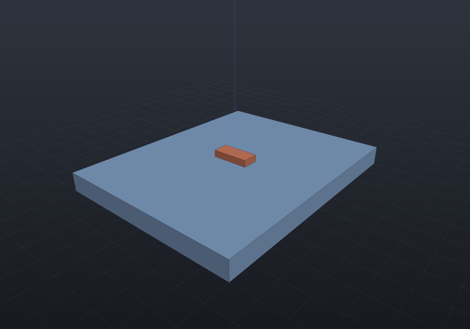
A file-referenced model is the other source — ComponentModel3D.FromFile("models/R_0805.step", placement) — and it travels as data ({ path, offset?, rotate?, scale? }, write-only-when-stated),
a byte-identical fixed point through the schematic and board files. Loading is an explicit act
(model.TryLoad(out var error) soft, model.Load() hard): a missing or unreadable file or an
.igs/.iges is RECORDED but refused
by name, never a data-load crash — so a data-only model that only references a path is honest
and complete for persistence and connectivity. A .wrl (VRML — KiCad’s default 3D model format)
loads through the mesh tier’s VrmlReader (the VRML97 IndexedFaceSet subset through the
Transform/DEF/USE scene graph), with the KiCad unit convention — 1 VRML unit = 0.1 inch =
2.54 mm — applied here, at the consumer that knows a component model’s .wrl is KiCad’s; the
reader itself reads coordinates verbatim, since VRML is unitless.
When the symbol and footprint disagree
A PinIdentity.Check names every mismatch. If a footprint were missing pad "8" and carried a
stray pad "99", the report would say so by number — pin '8' has no footprint pad,
footprint pad '99' is not a pin of the definition — so a wrong pairing fails loudly rather
than shipping a part whose copper does not match its schematic.
What the reader covers
The reader maps the common subset and NAMES anything else rather than mis-reading it:
- Symbol (
.kicad_sym): theReference/Footprintproperties, the unit sub-symbols (each<name>_<unit>_<style>kept as its ownSymbolinUnits, unit0common to every unit, the union of their pins the netlist terminals), graphicrectangle/circle/arc/polyline/text, andpins (electrical type →PinType, name, number, position, angle → direction, length). A bezier graphic, an alternate pin function, a De Morgan alternate body style (_1_2), or an electrical type with no exactPinTypeis ignored with a named diagnostic; two units disagreeing about one pin are reported by name (the first is kept). - Footprint (
.kicad_mod): SMD and plated through-hole pads of the standard shapes (circle/rect/roundrect/oval) with theirat/size/drill. A pad rotation (not carried by a footprint pad), atrapezoid/customshape, or an oval drill is approximated with a note. - 3D model (
.kicad_mod’s(model …)): the footprint’s(model "path" (offset (xyz …)) (rotate (xyz …)) (scale (xyz …)))becomes the definition’sModel— aFromFilereference carrying the path plus the placement (offset in mm, rotate in degrees, scale unitless). The file is NOT force-loaded (an empty library directory is normal); the reference is recorded and loaded on demand.
Generating a footprint from the datasheet (IPC-7351)
When no library carries the part, the land pattern comes from the component’s own datasheet
dimensions — Ipc7351 is a generator, the complement of the importers above. One formula
family serves every leaded shape: the outer land extent Z = Lmin + 2·J_toe + √(C² + F² + P²),
the inner gap G from the heel span, the land width X from the lead width — with the
toe/heel/side fillet goals per density level (Most/Nominal/Least, transcribed IPC-7351B
nominals, ⚠ verify against the standard for a production part). Covered: two-terminal chips (0603
imperial and larger), dual gullwing (SOIC/SSOP/TSSOP numbering), quad gullwing (QFP,
counter-clockwise from pin 1), SOT-23, and BGA grids with JEDEC row lettering (A…Y skipping
I/O/Q/S/X/Z, then AA…). A land whose inner gap closes — the pads would merge — is refused naming
the number, and StandardBodies carries common nominal bodies (⚠ the real part’s datasheet is
always the better input):
// A SOIC-8 and an 0805 land pattern from body dimensions alone — no library file anywhere.var soic8 = Ipc7351.DualGullwing("SOIC-8", StandardBodies.SoicNarrow, 8);var r0805 = Ipc7351.Chip("R0805", StandardBodies.Chip0805);Console.WriteLine($"SOIC-8: {soic8.Pads.Count} pads; 0805: {r0805.Pads.Count} pads");
// Density is a real trade: Most buys more solder fillet (a larger land), Least a denser board.foreach (var d in new[] { LandDensity.Least, LandDensity.Nominal, LandDensity.Most }){    var fp = Ipc7351.Chip("R0805", StandardBodies.Chip0805, new Ipc7351Options(Density: d));    var p2 = fp.Pads.Single(p => p.Number == "2");    Console.WriteLine($"0805 {d}: Z = {2 * (p2.Center.X + p2.Width / 2):0.00} mm");}
// The output IS a Footprint — it feeds a PartDefinition (and thence a board) directly, and the// pin/pad identity holds by construction.var part = new PartDefinition("IC", "U",    soic8.Pads.Select(p => new Pin(p.Number, PinType.Passive)), soic8);Console.WriteLine($"identity: {PinIdentity.Check(part).Ok}");
Courtyard and silkscreen are not part of a Footprint here — they derive downstream (the
silkscreen layer builds a courtyard from the pads). Filed by name: the small-chip goal row
(below 1608 metric), QFN/DFN and the other no-lead families, MELF, chip arrays, and thermal-pad
paste divisions.
Malformed input — a file that is not a KiCad symbol library or footprint, an unbalanced
parenthesis, an unterminated string; or an Eagle file handed to the wrong reader, or whose XML is
malformed — is refused by name (the StepReader/IgesReader rule). EDIF is later work (Eagle
.sch schematics and .brd boards both import, and IPC-7351 footprint generation and the VRML
(.wrl) reader landed — see above); IGES (.igs) 3D-model loading stays filed (refused by name,
the reference recorded).