The PCB fabrication drawing
The Gerbers and the Excellon drill program are what a board house machines from; the fabrication drawing is what a board house reads. It is the human- readable sheet that sits beside the fab data: the board outline at a fitted scale, a drill map with a symbol at every drilled feature, a drill table (a keyed legend) grouping the board’s holes, vias and through-hole pad drills by size, a layer stackup table, and a fabrication notes block — all on the shared engineering frame a mechanical drawing uses.
The one rule: it reads the board, it never edits it
A PcbFabricationSheet derives everything from the layout’s own public read surface — the board
outline, its holes, the placed vias, the stackup — so it cannot disagree with the board it
documents (the ECAD one-declaration rule, applied to a drawing). The drill table is the sharpest
form of that: its rows partition the board’s holes, vias and through-hole pad drills exactly,
so Σ count equals the number of drilled features and adding a hole (or a through-hole pad) adds
exactly one to its row. That is a closed-form oracle, not a picture.
The shared frame — the third consumer
A fabrication drawing is an engineering drawing, so its border and title block come from the same
DrawingFrame the mechanical drawing sheet and the
schematic sheet use — the three-band EngineeringTitleBlock on the
SheetLayers. Given the same paper and the same title-block fields, sheet.Frame().Compute()
is byte-identical to a mechanical DrawingSheet’s frame. That is the payoff of one shared
frame: a drawing and its fab drawing of one board cannot draw different furniture.
A drill map, a stackup and notes
A four-layer board with two mounting holes and a couple of via sizes, drawn on A3:
// A 4-layer board (60 x 40) with two Ø3.2 mounting holes and one Ø0.6 board via.var board = new PcbBoard(    [        new Vector2d(-30, -20), new Vector2d(30, -20),        new Vector2d(30, 20), new Vector2d(-30, 20),    ],    LayerStackup.FourLayer(copper: 0.035, prepreg: 0.2, core: 1.13),    holes:    [        new BoardHole(new Vector2d(-26, -16), 3.2, BoardHoleKind.Mounting),        new BoardHole(new Vector2d(26, 16), 3.2, BoardHoleKind.Mounting),        new BoardHole(new Vector2d(0, 15), 0.6, BoardHoleKind.Via),    ]);
// A through-hole header — its Ø0.9 plated pad drills join the SAME drill table as the board's// own holes and vias (an SMD part's lands would carry no drill and add no row).var sch = new Schematic("regulator");sch.Add("J1", new PartDefinition("HDR_1x2", "J",    [new Pin("1", PinType.Passive), new Pin("2", PinType.Passive)],    new Footprint("HDR254", [        Pad.ThroughHole("1", new Vector2d(-1.27, 0), pad: 1.6, drill: 0.9),        Pad.ThroughHole("2", new Vector2d(1.27, 0), pad: 1.6, drill: 0.9),    ])));
var layout = new PcbLayout(sch, board);// Placed vias in two sizes — they join the drill table with the board's own holes.layout.AddVia("GND", 8, 6, "Top", "Bottom", drill: 0.3, pad: 0.6);layout.AddVia("GND", -8, 6, "Top", "Bottom", drill: 0.3, pad: 0.6);layout.AddVia("GND", 0, -6, "Top", "Bottom", drill: 0.3, pad: 0.6);layout.AddVia("VIN", 12, -10, "Top", "Bottom", drill: 0.4, pad: 0.8);layout.Place("J1", 0, 0, rotationDegrees: 0, side: CopperSide.Top);
// The fabrication drawing — the shared engineering frame plus the fab content.var title = new TitleBlock{    Title = "REGULATOR PCB", DrawingNumber = "PCB-042", Author = "EngrCAD",    Revision = "A", Company = "ACME ELECTRONICS",};var sheet = new PcbFabricationSheet(layout, SheetFormat.A3, title);var drawing = sheet.Compute();
// The drill table partitions the board's holes, vias AND the header's through-hole pad drills://   Ø0.3 PTH x3, Ø0.4 PTH x1, Ø0.6 PTH x1, Ø0.9 PTH x2, Ø3.2 NPTH x2  — nine features, five sizes.var svg = drawing.ToSvg();   // also drawing.ToDxf(), drawing.ToPdf()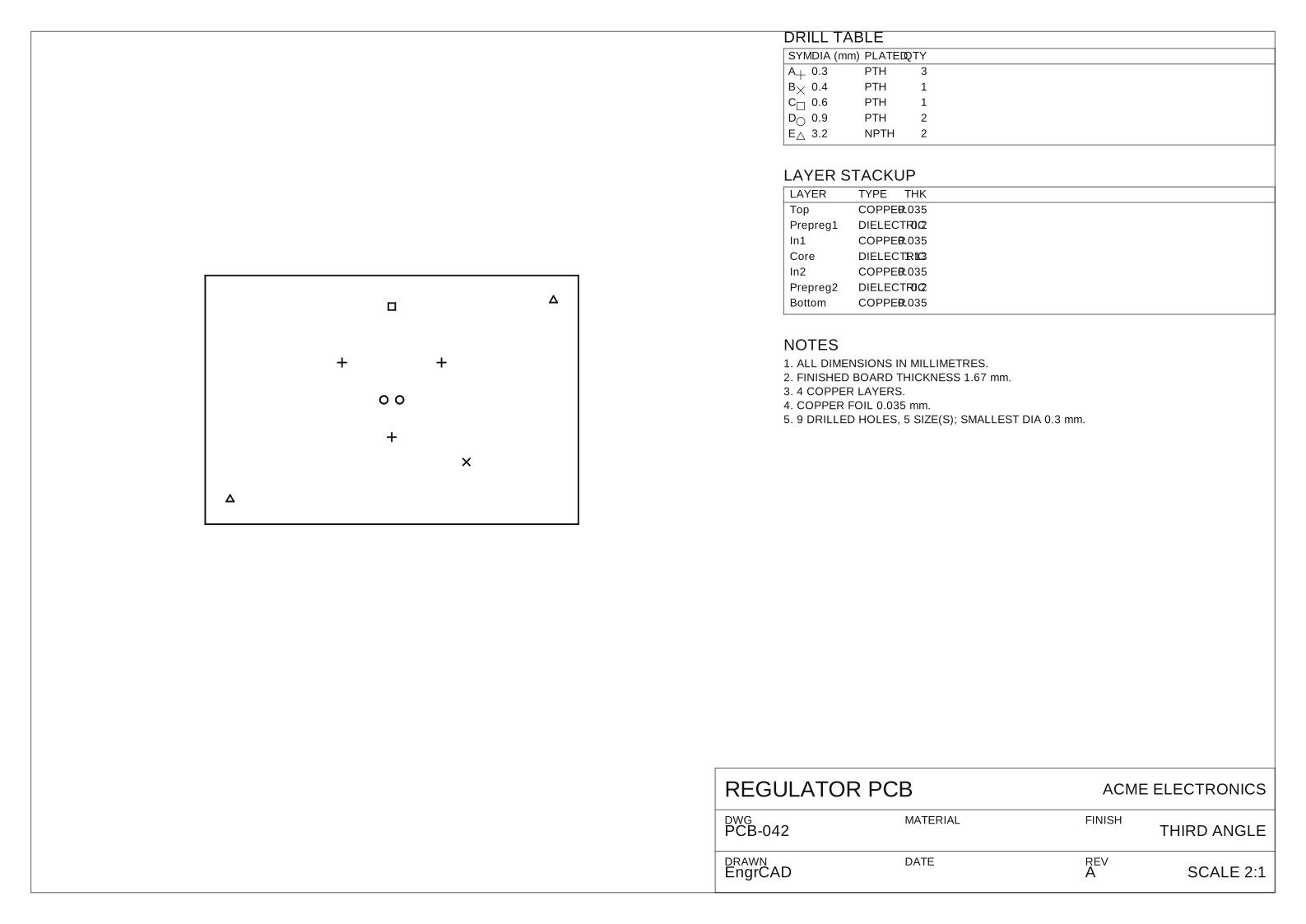
The drill table’s counts and diameters are the board’s own — the drawing is a view of the
layout’s drilled features, so it cannot omit a hole nor invent one. The same Compute() feeds
the SVG, DXF and PDF writers, so the three cannot disagree about the drawing.
The drill legend, and through-hole component pad drills
The drill table is a legend: its SYM column keys each size to a symbol — a letter
(A, B, …) beside its glyph, the same glyph the drill map draws at every hole of that size —
so a reader ties a marked hole back to its row. The glyphs come from PcbFabricationSheet’s
canonical, ordered symbol set (DrillGlyphPalette: plus, saltire, square, circle, triangle,
diamond, six-point asterisk, hexagon, down-triangle, pentagon), assigned by ascending diameter
(non-plated before plated at equal diameter), so the symbol assignment is a deterministic function
of the board. The letter is the always-distinct key; when a board carries more distinct sizes than
the palette has shapes the glyph cycles and the letter distinguishes the repeat. A board with
more distinct drill sizes than the A–Z alphabet holds (MaxLegendSizes = 26) is refused by
name — a real board carries a handful of drill sizes.
The partition covers through-hole component pad drills too, not just the board’s own holes and
vias. A through-hole pad has a drill; a surface-mount land does not — the same SMD-vs-through-hole
distinction the solder-paste stencil reads off the copper model — so a placed
header’s pads join the same (diameter, plated) partition (plated, PTH) while an SMD part contributes
no drill row.
Fabrication requirements: the notes the geometry cannot carry
The geometry states a thickness and a copper-layer count, but a board house also needs the base
material, the copper weight, the surface finish, the mask and legend colours, the IPC-6012 class,
and the minimum trace and clearance — none of which the geometry carries. A
PcbFabricationSpec states them, and the fabrication
drawing prints them write-only-when-stated: every field is optional, a stated field prints its
note, and an unstated one is simply absent — the drawing never invents a value. The spec rides in
the layout as layout truth (layout.WithFabrication(...), layout.Fabrication), the same kind
of thing the solder-mask / silkscreen / paste settings are, so it persists in the layout file
write-only-when-stated (a layout that states none saves byte-identically to a pre-spec one).
// A 2-layer board (60 x 40 x 1.6) — the geometry says nothing about material or finish.var board = new PcbBoard(    [        new Vector2d(-30, -20), new Vector2d(30, -20),        new Vector2d(30, 20), new Vector2d(-30, 20),    ],    thickness: 1.6,    holes:    [        new BoardHole(new Vector2d(-26, -16), 3.2, BoardHoleKind.Mounting),        new BoardHole(new Vector2d(26, 16), 3.2, BoardHoleKind.Mounting),    ]);
// The fabrication REQUIREMENTS the geometry cannot carry. Every field is optional — this spec// states a material, finish, copper weight, colours, class and minimum trace/clearance, and// leaves everything else (e.g. an impedance tolerance) to the fabricator's default.var layout = new PcbLayout(new Schematic("sensor"), board)    .WithFabrication(new PcbFabricationSpec    {        BaseMaterial = "FR-4",        FinishedThicknessMm = 1.6,        CopperWeightOz = 1,        SurfaceFinish = PcbSurfaceFinish.Enig,        SolderMaskColour = "Blue",        SilkscreenColour = "White",        Ipc6012Class = 2,        MinTraceWidthMm = 0.15,        MinClearanceMm = 0.15,        Notes = ["50 OHM CONTROLLED IMPEDANCE ON ROUTED NETS."],    });
var title = new TitleBlock{    Title = "SENSOR PCB", DrawingNumber = "PCB-108", Author = "EngrCAD", Company = "ACME",};var drawing = new PcbFabricationSheet(layout, SheetFormat.A3, title).Compute();
// The notes block now carries the stated requirements, e.g. "MATERIAL: FR-4.",// "SURFACE FINISH: ENIG.", "COPPER WEIGHT: 1 oz (35 um).", "FABRICATE TO IPC-6012 CLASS 2." —// each printed only because the spec states it.var svg = drawing.ToSvg();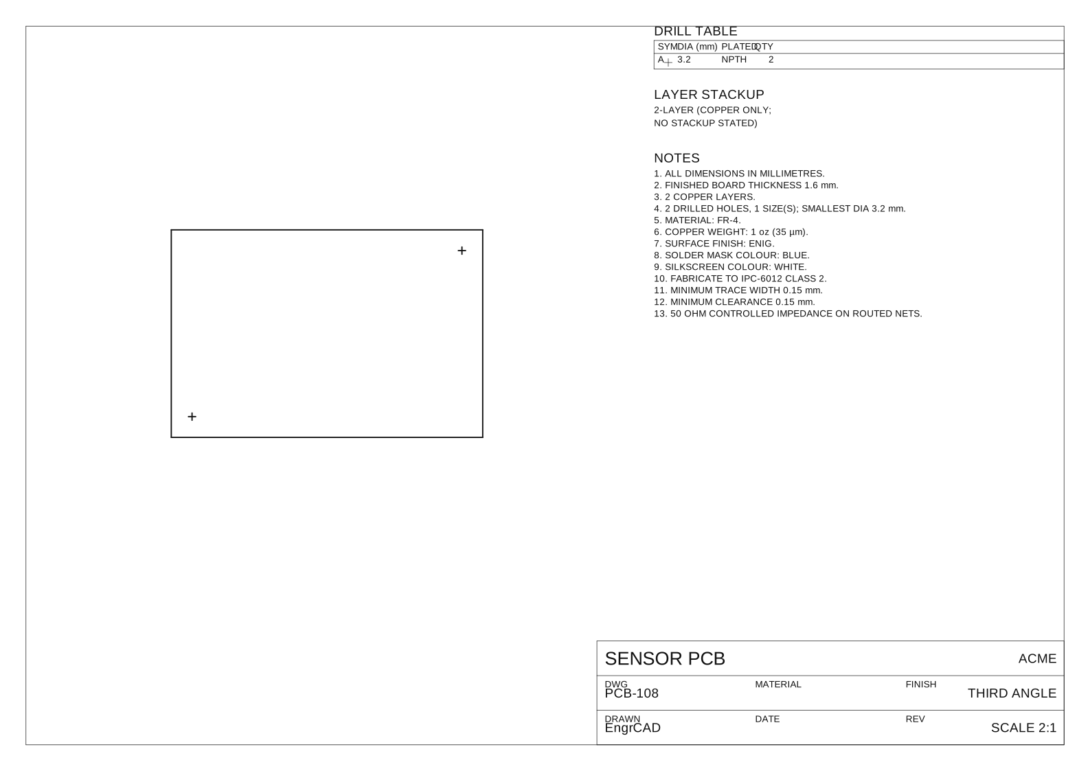
A stated finished thickness is authoritative: it is the delivered stackup thickness (copper and finish) a fabricator quotes to, so it replaces the modelled plate thickness in the finished- thickness note rather than printing a second one. With no spec, that note is the modelled thickness exactly as before — the drawing is byte-identical to one built before the spec existed.
A house standard from the catalogue
Typing the same fields for every board gets old, so StandardFabSpecs is a small catalogue of
common house specs — TwoLayerFr4Hasl, TwoLayerFr4Enig, FourLayerFr4Enig, FlexPolyimideEnig
— each an ordinary PcbFabricationSpec you pass to WithFabrication. It is the same
verify-against-datasheet pattern as StandardHoles / SheetMaterials: ⚠ nominal transcribed
figures — check them against your fabricator’s capability sheet. Because a catalogue entry is
an ordinary spec, it persists and drives the fab drawing through exactly the machinery above — there
is no second application path. The spec carries no layer count (that lives on the board’s stackup),
so the two 2-layer entries differ only by finish (HASL vs ENIG) and the 4-layer one is a
higher-reliability class-3 build; tweak any preset with a record with expression.
The per-layer plots — the sheet set beside the Gerbers
A fab package ships more than the Gerbers and the drill program: a board house also reads a
plot per layer — a human-readable sheet showing one copper / solder-mask / silkscreen /
solder-paste layer’s own geometry as line-work. PcbFabricationPlots.For(layout) produces that
set: one PcbLayerPlot per copper layer (in stackup order), then one per declared mask,
silk and paste side (write-only-when-stated, so a bare copper board plots just its copper layers).
Each plot consumes the copper model’s own regions — the same geometry the
Gerber exporter builds — so a plot and its Gerber cannot disagree about
what is on a layer; a copper plot draws exactly the PcbCopperModel’s features for that layer,
a mask plot the mask windows, a paste plot the SMD apertures, a silk plot the line-work. Each
plot rides the same shared frame (plot.Frame() is byte-identical to a fab drawing’s frame
at the same paper and fields), and a bottom-side layer is mirrored — plotted viewed from
the bottom, the way a fabricator looks at that side — with the plot stating its ViewSide and
Mirrored.
// A small 2-layer board with an SMD resistor and a through-hole header (copper on both layers),// with the solder mask declared so the mask sides plot too.var sch = new Schematic("blinky");var r = sch.Add("R1", new PartDefinition("R_0805", "R",    [new Pin("1", PinType.Passive), new Pin("2", PinType.Passive)],    new Footprint("R0805", [        Pad.Smd("1", new Vector2d(-1.0, 0), 1.2, 1.4),        Pad.Smd("2", new Vector2d(1.0, 0), 1.2, 1.4),    ])), "330");var j = sch.Add("J1", new PartDefinition("HDR_1x2", "J",    [new Pin("1", PinType.Passive), new Pin("2", PinType.Passive)],    new Footprint("HDR254", [        Pad.ThroughHole("1", new Vector2d(-1.27, 0), pad: 1.6, drill: 0.9),        Pad.ThroughHole("2", new Vector2d(1.27, 0), pad: 1.6, drill: 0.9),    ])));sch.Connect("VCC", j.Pin("1"), r.Pin("1"));sch.Connect("SIG", r.Pin("2"), j.Pin("2"));
var board = new PcbBoard(    [        new Vector2d(-15, -10), new Vector2d(15, -10),        new Vector2d(15, 10), new Vector2d(-15, 10),    ],    thickness: 1.6,    holes: [new BoardHole(new Vector2d(-12, -7), 3.0, BoardHoleKind.Mounting)]);var layout = new PcbLayout(sch, board);layout.Place("R1", 6, 2, rotationDegrees: 0, side: CopperSide.Top);layout.Place("J1", -6, -2, rotationDegrees: 30, side: CopperSide.Top);layout.WithMask(new PcbMaskSettings(Expansion: 0.05));
// Copper Top / Bottom, then mask Top / Bottom — four plots. Each names its layer and side.var plots = PcbFabricationPlots.For(layout, SheetFormat.A4,    new TitleBlock { Title = "BLINKY PCB", DrawingNumber = "PCB-001", Company = "ACME" });
// Render the TOP COPPER plot. plots[0].Compute() also has ToDxf() and ToPdf().var topCopper = plots[0];   // copper layers come first, in stackup ordervar svg = topCopper.Compute().ToSvg();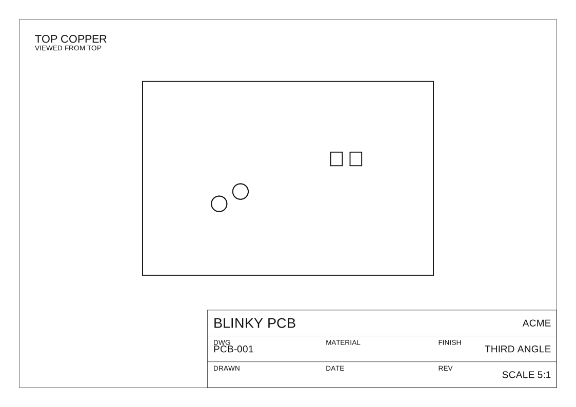
The bottom plots are the same geometry viewed from the other side: for a board point p,
bottomPlot.Compute().Project(p) maps to the same sheet Y as the top plot but a reflected X,
so the two are mirror images about the sheet — the fabrication convention that a bottom layer is
read looking through the board. Because a plot draws exactly its layer’s own regions, the plot’s
PlottedArea equals the copper model’s total region area for that layer — the plot is the
layer’s geometry, not a re-derivation.
var board = new PcbBoard(    [        new Vector2d(-30, -20), new Vector2d(30, -20),        new Vector2d(30, 20), new Vector2d(-30, 20),    ],    thickness: 1.6);
// Pick a house standard — then override just what differs (a black mask here).var spec = StandardFabSpecs.TwoLayerFr4Enig with { SolderMaskColour = "Black" };var layout = new PcbLayout(new Schematic("sensor"), board).WithFabrication(spec);
// It reaches the fab drawing through the same PcbFabricationSheet seam — no new drawing code.var notes = new PcbFabricationSheet(layout).Compute().Notes;if (!notes.Contains("SURFACE FINISH: ENIG."))    throw new Exception("the catalogue spec's finish should print on the fab drawing");if (!notes.Contains("SOLDER MASK COLOUR: BLACK."))    throw new Exception("the override should carry through");
// And it persists like any other spec — a save -> load -> save fixed point.if (PcbLayout.Load(layout.Save()).Save() != layout.Save())    throw new Exception("a catalogue spec should round-trip like any other");
// Every catalogue entry's stated minimums conform to the IPC class it claims.foreach (var (name, s) in StandardFabSpecs.All)    if (!DrcRuleSet.CheckSpec(s).Conforms)        throw new Exception($"{name} contradicts its own IPC class");Console.WriteLine($"catalogue: {StandardFabSpecs.All.Count} house specs, all class-conforming");