The board and its parts
Stage 2 of the ECAD campaign turns a schematic into a board: a plate
with a copper stackup, a set of placed components, and the 3D assembly that falls out of them.
The load-bearing rule carries over — one declaration produces both. The schematic graph is
the single source; the board copper, the footprint placement and the 3D bodies all derive
from it, so a pin and its pad are one identity (pin 1 ↔ pad 1) and nothing can drift.
A board is geometry the kernel already builds
A PcbBoard is a polygon outline, a thickness, a copper stackup (top and bottom copper by
default, N layers for a multilayer board) and its own holes (mounting holes and vias). The
plate is built with the ordinary Shape API — the outline extruded, the holes drilled — so
it is an exact B-Rep with a closed-form volume:
plate volume = outline area × thickness − Σ πr² × thickness
which is the oracle the tests hold it against (the tessellated volume approaches it from below by each round hole’s inscribed-polygon chord deficit).
Placing components derives copper, drills and bodies
A PcbLayout is a schematic, a board, and a list of placements — each a (x, y, rotation, side)
pose naming a component the schematic declares. From that one declaration a placement derives:
- its footprint pads projected onto the correct copper layer at the placed pose (an SMD pad lands on its side’s copper; a through-hole pad appears on every layer);
- its through-hole pads drilled into the plate (the same hole serves both faces);
- for a component whose definition carries a 3D
Body, its body posed into the assembly.
A bottom-side placement is a genuine reflection: the body hangs below the board and its
through-holes keep the same world (x, y). The reflection lives on the component’s part
transform and its square is the identity (Mirror(Mirror(x)) == x), so the board’s own +Z — world
up — is never touched (the FlipX-not-FlipZ doctrine: the reflection is spent on the part, the
pose stays a proper frame).
The one-declaration identity check
PcbLayout.Check() is the geometric lift of the schematic’s pin-counting identity: every pin of
every placed component resolves to exactly one placed pad at a known copper location. The two
counts (PlacedPinCount == PlacedPadCount, every pin covered once) are exposed so the identity can
be asserted numerically, and the lists it splits into — a pad with no pin, a pin with no pad, a
pad off the board — name which way it failed. A net’s pins then resolve to specific copper regions
(PadsOfNet), which is the seam DRC and routing (later stages) consume.
// A schematic — the single source (bodies + footprints named once, instanced as components).var resistor = new PartDefinition("R_0805", "R",    new[] { new Pin("1", PinType.Passive), new Pin("2", PinType.Passive) },    new Footprint("R0805", new[] {        Pad.Smd("1", new Vector2d(-1.0, 0), 1.2, 1.4),        Pad.Smd("2", new Vector2d(1.0, 0), 1.2, 1.4),    }),    body: () => Shape.Box(2.0, 1.25, 0.6).Translate(0, 0, 0.3));var header = new PartDefinition("HDR_1x2", "J",    new[] { new Pin("1", PinType.Passive), new Pin("2", PinType.Passive) },    new Footprint("HDR254", new[] {        Pad.ThroughHole("1", new Vector2d(-1.27, 0), pad: 1.6, drill: 0.9),        Pad.ThroughHole("2", new Vector2d(1.27, 0), pad: 1.6, drill: 0.9),    }),    body: () => Shape.Box(5.08, 2.54, 4.0).Translate(0, 0, 2.0));
var sch = new Schematic("blinky");var r = sch.Add("R1", resistor, "330");var j = sch.Add("J1", header);sch.Connect("VCC", j.Pin("1"), r.Pin("1"));sch.Connect("SIG", r.Pin("2"), j.Pin("2"));
// A board, and the components placed on it.var board = new PcbBoard(    new[] {        new Vector2d(-20, -15), new Vector2d(20, -15),        new Vector2d(20, 15), new Vector2d(-20, 15),    },    thickness: 1.6,    holes: new[] {        new BoardHole(new Vector2d(-17, -12), 3.0, BoardHoleKind.Mounting),        new BoardHole(new Vector2d(17, 12), 3.0, BoardHoleKind.Mounting),    });
var layout = new PcbLayout(sch, board);layout.Place("R1", 6, 0, rotationDegrees: 0, side: CopperSide.Top);layout.Place("J1", -8, 0, rotationDegrees: 90, side: CopperSide.Top);
// The identity check — the geometric lift of the schematic's pin count.var check = layout.Check();if (!check.Ok) throw new Exception(check.ToString());Console.WriteLine($"pins {check.PlacedPinCount} == pads {check.PlacedPadCount}, identity holds: {check.IdentityHolds}");
// VCC's two pins resolve to two copper locations.var vcc = layout.Schematic.Nets.First(n => n.Name == "VCC");foreach (var pad in layout.PadsOfNet(vcc))    Console.WriteLine($"  VCC -> {pad.Name} at ({pad.World.X:g4}, {pad.World.Y:g4})");
// The plate volume matches the closed form (a through-hole header drilled two 0.9 mm holes).Console.WriteLine($"plate volume (closed form): {layout.ExpectedPlateVolume():g6} mm^3");
// The layout is a byte-identical save -> load -> save fixed point.var jsonText = layout.Save();if (PcbLayout.Load(jsonText, new PartLibrary()).Save() != jsonText)    throw new Exception("the layout is not a persistence fixed point");
The board as an assembly
ToAssembly() builds the drilled plate plus one occurrence per placed component whose definition
carries a body — the same Assembly / PartInstance flattening the viewer, the BOM and every
exporter already consume. The 3D render below is that assembly:
var resistor = new PartDefinition("R_0805", "R",    new[] { new Pin("1", PinType.Passive), new Pin("2", PinType.Passive) },    new Footprint("R0805", new[] {        Pad.Smd("1", new Vector2d(-1.6, 0), 1.2, 1.4),        Pad.Smd("2", new Vector2d(1.6, 0), 1.2, 1.4),    }),    body: () => Shape.Box(3.2, 1.6, 0.6).Translate(0, 0, 0.3));var led = new PartDefinition("LED_1206", "D",    new[] { new Pin("A", "anode", PinType.Passive), new Pin("K", "cathode", PinType.Passive) },    new Footprint("LED1206", new[] {        Pad.Smd("A", new Vector2d(-1.6, 0), 1.4, 1.6),        Pad.Smd("K", new Vector2d(1.6, 0), 1.4, 1.6),    }),    body: () => Shape.Cylinder(1.4, 1.2).Translate(0, 0, 0.6));var header = new PartDefinition("HDR_1x3", "J",    new[] { new Pin("1", PinType.Passive), new Pin("2", PinType.Passive), new Pin("3", PinType.Passive) },    new Footprint("HDR254", new[] {        Pad.ThroughHole("1", new Vector2d(-2.54, 0), 1.6, 0.9),        Pad.ThroughHole("2", new Vector2d(0.0, 0), 1.6, 0.9),        Pad.ThroughHole("3", new Vector2d(2.54, 0), 1.6, 0.9),    }),    body: () => Shape.Box(7.62, 2.54, 6.0).Translate(0, 0, 3.0));
var sch = new Schematic("blinky");sch.Add("R1", resistor, "330");sch.Add("D1", led);sch.Add("J1", header);
var board = new PcbBoard(    new[] {        new Vector2d(-22, -16), new Vector2d(22, -16),        new Vector2d(22, 16), new Vector2d(-22, 16),    },    thickness: 1.6,    holes: new[] {        new BoardHole(new Vector2d(-18, -12), 3.2, BoardHoleKind.Mounting),        new BoardHole(new Vector2d(18, -12), 3.2, BoardHoleKind.Mounting),        new BoardHole(new Vector2d(-18, 12), 3.2, BoardHoleKind.Mounting),        new BoardHole(new Vector2d(18, 12), 3.2, BoardHoleKind.Mounting),    });
var layout = new PcbLayout(sch, board);layout.Place("R1", 2, 6, 0, CopperSide.Top);layout.Place("D1", 10, 6, 0, CopperSide.Top);layout.Place("J1", -12, 0, 0, CopperSide.Top);
var scene = new Scene();scene.AddTab("Board").Add(layout.ToAssembly());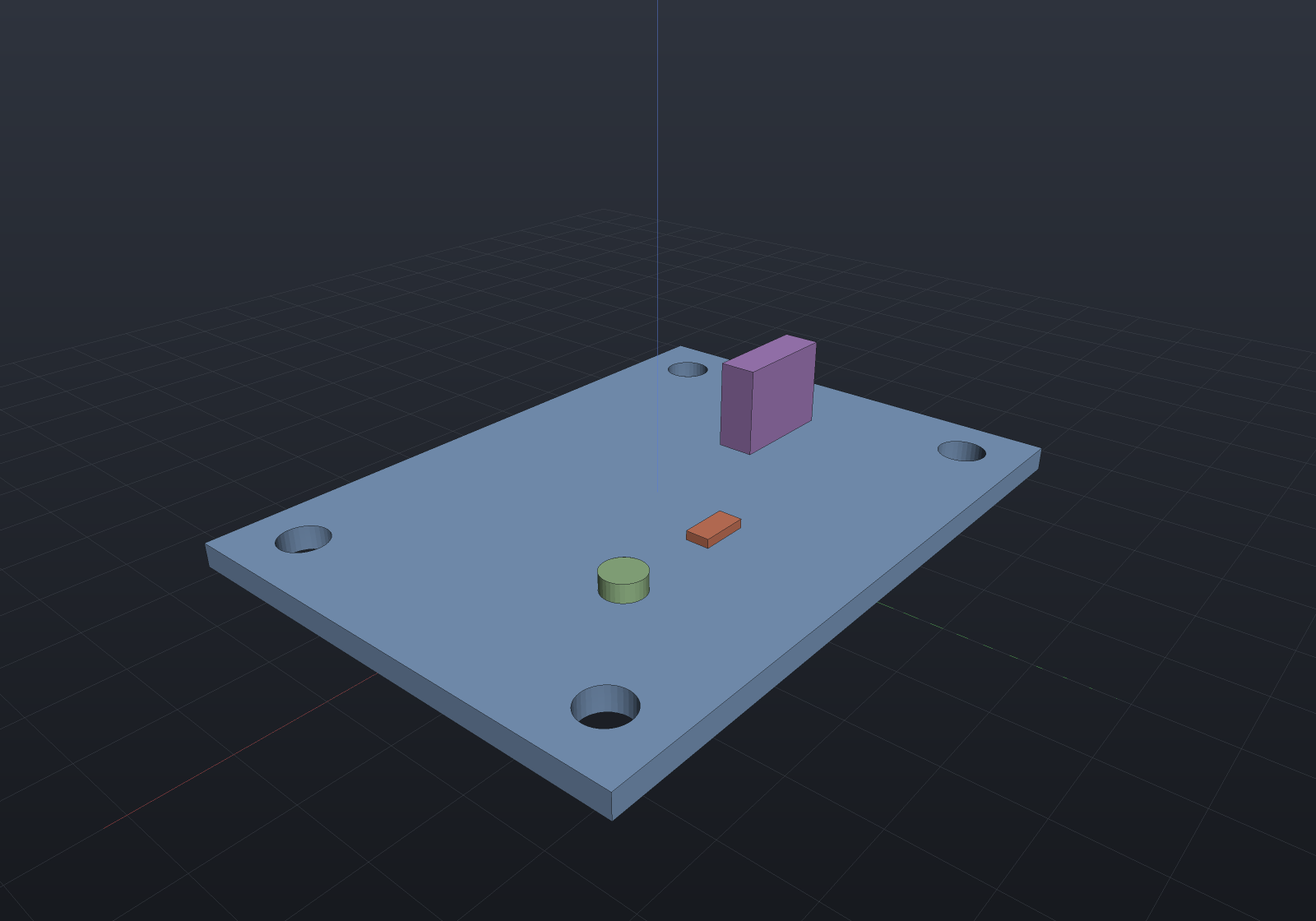
Multilayer stackups and embedded components
A board is more than two copper layers, and a component is not always on a surface. A full
LayerStackup is an ordered list of copper and dielectric layers, each with a thickness
(copper–dielectric–…–copper — the standard 2 / 4 / 6-layer builds). The board is extruded through
the whole build-up, and each copper plane’s z is derived from it: the top and bottom coppers
sit at the two faces, the inner coppers between.
A component placed with Embed(reference, layer, x, y) seats on an inner copper layer — inside
the board, in a cavity milled into the plate. Two embedding styles:
- Enclosed (the default): a buried, internal cavity. The build-up above and below stays intact, so the die has no external access and its body is strictly inside the board volume.
- Open cavity: a well milled down from the placement’s face, so the component is accessible and the well breaks that surface.
The cavity is sized to the component’s footprint (and body) plus a stated clearance, and its volume
comes off the plate exactly (footprint-plus-clearance area × depth). The one-declaration
identity holds across layers: an embedded component’s pads map to their inner layer’s copper, the
identity Check still passes, and the copper DRC is fully N-layer aware.
// A 4-layer build-up: Top / prepreg / In1 / core / In2 / prepreg / Bottom.var stackup = LayerStackup.FourLayer(copper: 0.035, prepreg: 0.2, core: 1.13);Console.WriteLine($"total thickness = {stackup.TotalThickness:g4} mm (== the sum of every layer)");foreach (var c in stackup.Coppers)    Console.WriteLine($"  copper '{c.Name}' at z = {c.Z:g5} mm");
var board = new PcbBoard(    new[] { new Vector2d(-25, -20), new Vector2d(25, -20), new Vector2d(25, 20), new Vector2d(-25, 20) },    stackup);
// A die (body + footprint) to bury on an inner layer, and a surface resistor.var die = new PartDefinition("DIE", "U",    new[] { new Pin("1", PinType.Passive), new Pin("2", PinType.Passive) },    new Footprint("DIE_SMD", new[] {        Pad.Smd("1", new Vector2d(-1.5, 0), 1.4, 2.0),        Pad.Smd("2", new Vector2d(1.5, 0), 1.4, 2.0),    }),    body: () => Shape.Box(4.0, 2.5, 0.5).Translate(0, 0, 0.25));var res = new PartDefinition("R_0805", "R",    new[] { new Pin("1", PinType.Passive), new Pin("2", PinType.Passive) },    new Footprint("R0805", new[] {        Pad.Smd("1", new Vector2d(-1.0, 0), 1.2, 1.4),        Pad.Smd("2", new Vector2d(1.0, 0), 1.2, 1.4),    }),    body: () => Shape.Box(2.0, 1.25, 0.5).Translate(0, 0, 0.25));
var sch = new Schematic("stack");var u1 = sch.Add("U1", die);var r1 = sch.Add("R1", res);sch.Connect("A", u1.Pin("1"), r1.Pin("1"));sch.Connect("B", u1.Pin("2"), r1.Pin("2"));
var layout = new PcbLayout(sch, board);layout.Embed("U1", "In2", 0, 0, cavityClearance: 0.15);   // buried on the inner layer In2layout.Place("R1", 14, 0, 0, CopperSide.Top);             // on the surface
// The enclosed cavity removes exactly its pocket, and the die is buried inside the board volume.var cavity = layout.Cavities().Single();Console.WriteLine($"cavity removes {cavity.RemovedVolume:g4} mm^3, buried z in [{cavity.ZLow:g3}, {cavity.ZHigh:g3}]");Console.WriteLine($"plate volume = {layout.ExpectedPlateVolume():g6} mm^3");
// The pin-count identity still holds across layers; U1's pads land on the inner copper.var check = layout.Check();if (!check.Ok) throw new Exception(check.ToString());Console.WriteLine($"identity holds across layers: {check.IdentityHolds}");var in2 = layout.CopperLayers().First(l => l.Name == "In2");Console.WriteLine($"In2 copper carries: {string.Join(", ", in2.Pads.Select(p => p.Name))}");
The section render below cuts the same idea through the middle, revealing the die sitting in its cavity between the copper layers:
// Look edge-on at the y = 0 cut face, so the section reveals the buried die.var camera = new CameraState(Math.PI / 2 - 0.55, 0.28, 52, (0, 0, 2.7));
// A thick illustrative build-up so the section reads (total ≈ 5.4 mm).var stackup = LayerStackup.FourLayer(copper: 0.1, prepreg: 0.5, core: 4.0);var board = new PcbBoard(    new[] { new Vector2d(-22, -13), new Vector2d(22, -13), new Vector2d(22, 13), new Vector2d(-22, 13) },    stackup);
// A die whose body is the cavity's whole depth, buried on the inner layer In2.var die = new PartDefinition("DIE", "U",    new[] { new Pin("1", PinType.Passive), new Pin("2", PinType.Passive) },    new Footprint("DIE", new[] {        Pad.Smd("1", new Vector2d(-2.2, 0), 1.6, 2.4),        Pad.Smd("2", new Vector2d(2.2, 0), 1.6, 2.4),    }),    body: () => Shape.Box(6.0, 4.0, 3.0).Translate(0, 0, 1.5));var res = new PartDefinition("R_0805", "R",    new[] { new Pin("1", PinType.Passive), new Pin("2", PinType.Passive) },    new Footprint("R0805", new[] {        Pad.Smd("1", new Vector2d(-1.0, 0), 1.2, 1.4),        Pad.Smd("2", new Vector2d(1.0, 0), 1.2, 1.4),    }),    body: () => Shape.Box(2.0, 1.25, 0.6).Translate(0, 0, 0.3));
var sch = new Schematic("stack");var u1 = sch.Add("U1", die);var r1 = sch.Add("R1", res);sch.Connect("A", u1.Pin("1"), r1.Pin("1"));sch.Connect("B", u1.Pin("2"), r1.Pin("2"));
var layout = new PcbLayout(sch, board);layout.Embed("U1", "In2", 0, 0, cavityClearance: 0.2);   // buried, enclosed, in an internal cavitylayout.Place("R1", 16, 0, 0, CopperSide.Top);            // proud on the top surface
var scene = new Scene();scene.AddTab("Board").Add(layout.ToAssembly());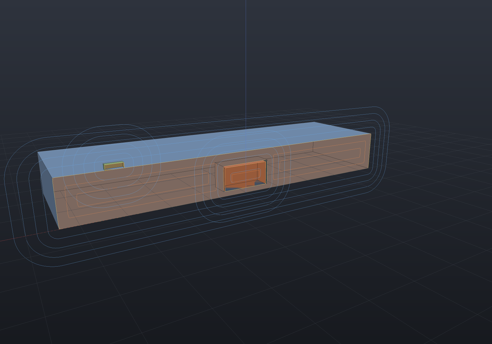
An embedded component’s cavity wall is a milled edge, so other copper on its seat layer must clear
it (DrcRule.CavityClearance), and clearance / shorts are checked per copper layer including the
inner ones. A net whose pads sit on different layers is joined by a via — see below.
Vias and cross-layer connectivity
A via is a net-carrying, plated cross-layer connection: a drilled, plated hole at (x, y)
spanning the copper layers [from, to], with an annular copper pad on every layer it touches. A
signal via transitions a routed trace between layers; a stitching via ties a plane — either way it
belongs to a net, so a via with no net is refused by name.
The via type is derived from the span, never stored twice: outer-face to outer-face is a
Through via, an outer face to an inner layer is Blind, buried between inner layers is Buried,
and a single dielectric hop (adjacent copper layers) is a Microvia.
The engine underneath is the one an autorouter reuses — a per-net connectivity graph. Two copper features join when they touch on the same layer (an exact region intersection) or are the two ends of a via (a plated barrel across the layers). A net is connected when all its pads lie in one component. This is the real answer to “a net whose pads sit on different layers” — a via that touches each is a genuine connection, not an unrouted ratsnest:
// A 4-layer board: copper planes Top / In1 / In2 / Bottom.var stackup = LayerStackup.FourLayer(copper: 0.035, prepreg: 0.2, core: 1.13);var board = PcbBoard.Rectangle(30, 20, stackup);
// A round pad, instanced on the top and on the bottom, wired into one net — a signal that has to// change layers to get from one to the other.var pad = new PartDefinition("PAD", "U",    new[] { new Pin("1", PinType.Passive) },    new Footprint("PAD", new[] { Pad.Smd("1", new Vector2d(0, 0), 1.2, 1.2, PadShape.Round) }));
var sch = new Schematic("stitch");var top = sch.Add("U1", pad);var bot = sch.Add("U2", pad);sch.Connect("SIG", top.Pin("1"), bot.Pin("1"));
var layout = new PcbLayout(sch, board);layout.Place("U1", 0, 0, side: CopperSide.Top);      // SIG on the top copperlayout.Place("U2", 0, 0, side: CopperSide.Bottom);   // SIG on the bottom copper
// Before any via, SIG's two pads sit on different layers — an UNROUTED ratsnest.Console.WriteLine($"before the via: SIG connected = {layout.IsNetConnected("SIG")}, "    + $"ratsnest = [{string.Join(", ", PcbDrc.Check(layout).Ratsnest)}]");
// A via ties the two layers. Its type is DERIVED from the span (Top..Bottom is a through via),// and it touches every copper layer it crosses.var stitch = new Via("SIG", 0, 0, "Top", "Bottom", DrillDiameter: 0.4, PadDiameter: 1.0);Console.WriteLine($"via Top..Bottom is a {layout.ViaTypeOf(stitch)} via touching "    + $"[{string.Join(", ", layout.ViaLayers(stitch))}]");layout.WithVia(stitch);
// Now the via's annular pads touch each pad — SIG is CONNECTED, and its ratsnest is empty.var connectivity = layout.Connectivity();Console.WriteLine($"after the via:  SIG connected = {connectivity.Of("SIG").IsConnected}, "    + $"ratsnest = [{string.Join(", ", connectivity.Unrouted)}]");
// The DRC catches a via with too thin an annular ring — a via IS a drilled pad, so (pad - drill)/2// must clear the minimum annular ring (0.15 mm by default).var check = new PcbLayout(new Schematic("drc"), board);check.AddVia("N", 8, 5, "Top", "Bottom", drill: 0.5, pad: 0.6);   // ring (0.6 - 0.5)/2 = 0.05 mmforeach (var v in PcbDrc.Check(check).OfRule(DrcRule.AnnularRing))    Console.WriteLine($"DRC: {v.Message}");
Because a via pad is ordinary copper and a via drill is a drilled hole, the general DRC rules reach
them for free — a via pad to different-net copper rides the copper-clearance rule, a via drill to
different-net copper the drill-to-copper rule, and a same-net via touching its own copper is the
intended connection and is never flagged (the one-declaration identity). The one genuinely new via
rule is via-to-via (DrcRule.ViaToVia): the minimum web between two drilled holes, applied to
all via pairs regardless of net (a manufacturing spacing). Vias are layout truth, so they
round-trip in the layout file; a via-free layout saves byte-identically.
Exploding the stack
The reason a full LayerStackup — copper AND dielectric, each with a thickness — is worth carrying
is that the board is then a sandwich the kernel knows how to take apart. ToExplodedAssembly()
slices the plate into one slab per physical layer (a dielectric core, or a thin copper film)
and assembles them with the placed components, fanned along the stackup normal. It is the
sibling of ToAssembly() (the board as one part) and rides the same Assembly / Occurrence
machinery, so the ordinary exploded-view slider and ExplodeTrack animate it with no new code.
Every decision is fixed by the fact that a PCB’s one interesting relationship is its z-stacking:
- The layers fan up from the bottom layer as the datum (it stays put — the natural datum, since
the stackup itself accumulates from the bottom face at z = 0). A layer’s offset is
stackup-normal · gap · rank, counting rank from the bottom, so stack order is explode order: a layer above another when assembled is above it when exploded, and because the offset adds to the layer’s original (contiguous) position,gapis the clean empty gap between consecutive layers whatever their thickness. - Surface components lift off their face — a top part up clear of the fan, a bottom part down below the datum. Pure Z.
- Embedded components come out of their cavity along Z first, then spread aside — an
Occurrence.ExplodePathdogleg whose first leg is pure ±normal (straight out of the cavity) and whose final offset carries a lateral step, so the die does not tunnel straight up through the layers above it (a diagonal reads as insert at an angle).
The slabs are disjoint, tile the stackup z-range exactly, and — being the outline drilled by every
through hole and milled by every cavity — their union is the plate: Σ slab volume equals
ExpectedPlateVolume(). At explode factor 0 the whole thing is the assembled board (each
component’s world transform is bit-identical to ToAssembly’s), so the animation genuinely opens
from the board and closes back to it.
// A thick illustrative 4-layer build-up so the fanned slabs read (total ≈ 5.4 mm).var stackup = LayerStackup.FourLayer(copper: 0.1, prepreg: 0.5, core: 4.0);var board = new PcbBoard(    new[] { new Vector2d(-22, -14), new Vector2d(22, -14), new Vector2d(22, 14), new Vector2d(-22, 14) },    stackup,    holes: new[] {        new BoardHole(new Vector2d(-18, -10), 3.0, BoardHoleKind.Mounting),        new BoardHole(new Vector2d(18, 10), 3.0, BoardHoleKind.Mounting),    });
var die = new PartDefinition("DIE", "U",    new[] { new Pin("1", PinType.Passive), new Pin("2", PinType.Passive) },    new Footprint("DIE", new[] {        Pad.Smd("1", new Vector2d(-2.2, 0), 1.6, 2.4),        Pad.Smd("2", new Vector2d(2.2, 0), 1.6, 2.4),    }),    body: () => Shape.Box(6.0, 4.0, 3.0).Translate(0, 0, 1.5));var res = new PartDefinition("R_0805", "R",    new[] { new Pin("1", PinType.Passive), new Pin("2", PinType.Passive) },    new Footprint("R0805", new[] {        Pad.Smd("1", new Vector2d(-1.0, 0), 1.2, 1.4),        Pad.Smd("2", new Vector2d(1.0, 0), 1.2, 1.4),    }),    body: () => Shape.Box(2.0, 1.25, 0.6).Translate(0, 0, 0.3));
var sch = new Schematic("stack");var u1 = sch.Add("U1", die);var r1 = sch.Add("R1", res);sch.Connect("A", u1.Pin("1"), r1.Pin("1"));sch.Connect("B", u1.Pin("2"), r1.Pin("2"));
var layout = new PcbLayout(sch, board);layout.Embed("U1", "In2", 0, 0, cavityClearance: 0.2);   // a die buried between the copper layerslayout.Place("R1", 15, 0, 0, CopperSide.Top);            // a resistor proud on top
// Slice the board into per-layer slabs and fan them along the stackup normal.var assembly = layout.ToExplodedAssembly();
var scene = new Scene();scene.AddTab("Board").Add(assembly);
// Sequence it: the layers fan open first, the surface part lifts, and the buried die comes out// LAST — straight up out of its cavity, then aside — once the layers above it have cleared.var track = new ExplodeTrack(scene, deriveOffsets: false);foreach (var occurrence in assembly.Occurrences){    if (occurrence.Name == "U1") track.Stagger(occurrence, 0.55, 1.0);    else if (occurrence.Name == "R1") track.Stagger(occurrence, 0.35, 0.85);    else track.Stagger(occurrence, 0.0, 0.6);}var animation = new Animation(durationSeconds: 5, AnimationEasing.Smoothstep).With(track);
deriveOffsets: false keeps the offsets ToExplodedAssembly computed (the generic
Assembly.AutoExplode would derive a mechanical radial explode instead, and would move the datum
layer). The offsets are pure geometry, so this — like AutoExplode — is off-the-render-thread work;
evaluating the animation is then matrices only, the instance count and order independent of the
factor.
Copper pours (ground planes)
A copper pour floods a layer with copper on one net — a ground plane, a power plane, a poured
fill. It is layout truth (a plane is part of the design), so a CopperPour derives
into copper features the DRC and the connectivity engine read exactly
like any other copper: a GND pour joins every GND pad it touches, so the GND ratsnest empties.
The fill region is exact and the tamper-mesh construction — the board area (or a stated outline), inset from the edge, minus every other-net copper and drill grown by the clearance, minus a thermal-relief annulus around each same-net through-hole pad (bridged by spokes). So the pour clears every other net by construction and a poured board passes the DRC:
// A through-hole part (GND on pin 1) and an SMD part (GND on pin 1), spread across the board.PartDefinition Header() => new("HDR", "J",    new[] { new Pin("1", PinType.Passive), new Pin("2", PinType.Passive) },    new Footprint("HDR_fp", new[] {        Pad.ThroughHole("1", new Vector2d(0, 0), pad: 1.8, drill: 1.0),        Pad.ThroughHole("2", new Vector2d(4, 0), pad: 1.8, drill: 1.0) }));PartDefinition Res() => new("R", "R",    new[] { new Pin("1", PinType.Passive), new Pin("2", PinType.Passive) },    new Footprint("R_fp", new[] {        Pad.Smd("1", new Vector2d(-0.8, 0), 1.0, 1.0), Pad.Smd("2", new Vector2d(0.8, 0), 1.0, 1.0) }));
var sch = new Schematic("pour-demo");var j = sch.Add("J1", Header()); var r = sch.Add("R1", Res());sch.Connect("GND", j.Pin("1"), r.Pin("1"));     // a THT GND pin and an SMD GND pin, far apartsch.Connect("SIG", j.Pin("2"), r.Pin("2"));
var board = new PcbBoard(new[] {    new Vector2d(-15, -10), new Vector2d(15, -10), new Vector2d(15, 10), new Vector2d(-15, 10) }, 1.6);var layout = new PcbLayout(sch, board);layout.Place("J1", 0, 0);          // J1.1 (GND, THT) at the origin — gets a thermal relieflayout.Place("R1", -10, 0);        // a second GND pad
Console.WriteLine($"before pour: GND connected = {layout.Connectivity().Of("GND").IsConnected}");
layout.AddPour(new CopperPour("GND", "Top"));   // default: four-spoke thermal relief on THT pads
var gnd = layout.Connectivity().Of("GND");var rules = DrcRuleSet.Default with { MinAcuteAngleDegrees = 45 };   // a realistic acid-trap thresholdvar report = PcbDrc.Check(layout, rules);var model = PcbCopperModel.FromLayout(layout);
// The relief: a point in the annular gap between the spokes carries NO copper, yet the THT pad is// still connected to the plane through the spokes.bool gapIsAir = !model.Copper.Any(f => f.Layer == "Top" && f.Region.Contains(new Vector2d(1.1, 0)));
Console.WriteLine($"after pour:  GND connected = {gnd.IsConnected}, ratsnest = [{string.Join(", ", report.Ratsnest)}]");Console.WriteLine($"THT relief gap is air: {gapIsAir}; DRC violations: {report.Violations.Count}");
if (!gnd.IsConnected || report.Ratsnest.Contains("GND") || !report.Ok || !gapIsAir)    throw new Exception("a GND pour must connect every GND pin (incl. through spokes) and stay DRC-clean");
Thermal relief keeps a same-net through-hole pad solderable: instead of flooding over it (which
would sink all its heat into the plane), the pour leaves an annular air gap around the pad bridged by
thin radial spokes (four on the diagonals, by default). The pad stays connected through the spokes
and relieved by the gap — asserted both ways above. SMD pads and vias are direct-connected
(flooded); ThermalRelief.None floods a through-hole pad too. Spokes meet the plane at ~90° corners,
so a poured board with thermal reliefs wants an acid-trap threshold at or below 90° (a realistic
board sets it well under 90° regardless).
A PourFill.Hatched variant intersects the fill with a crosshatch grid — the region ∩ a line
pattern — for a lighter, more flexible plane. Dead copper — a piece of the pour the net cannot
reach, walled off by other-net copper — is removed by default (kept only when
DeadCopper = DeadCopperPolicy.Keep) and always reported (PouredPour.DeadCopperArea). A pour
exports to Gerber as a G36/G37 region fill and round-trips, and rides in
the layout file (write-only-when-stated, so a pour-free layout is byte-identical).
Priority resolves where two pours overlap. Two different-net pours flooding the same area would
short; CopperPour.Priority makes the higher-priority pour fill first and keep its copper, so the
lower-priority one is carved back by its own clearance around it (same-net pours merge). Ties break by
declaration order, and a single pour — or pours that do not overlap — are unaffected, so it changes
only the case that would otherwise short:
PartDefinition Sq(string n) => new(n, "R",    new[] { new Pin("1", PinType.Passive), new Pin("2", PinType.Passive) },    new Footprint(n + "_fp", new[] {        Pad.Smd("1", new Vector2d(-1, 0), 1, 1, PadShape.Rectangular),        Pad.Smd("2", new Vector2d(1, 0), 1, 1, PadShape.Rectangular) }));
var sch = new Schematic("pp");var g = sch.Add("G", Sq("G")); var v = sch.Add("V", Sq("V"));sch.Connect("GND", g.Pin("1"), g.Pin("2"));sch.Connect("VCC", v.Pin("1"), v.Pin("2"));var board = new PcbBoard(new[] {    new Vector2d(-20, -15), new Vector2d(20, -15), new Vector2d(20, 15), new Vector2d(-20, 15) }, 1.6);var layout = new PcbLayout(sch, board);layout.Place("G", -15, 0); layout.Place("V", 15, 0);
// GND covers the left+centre, VCC the centre+right — overlapping in x ∈ [-3, 3]. GND wins the overlap.Vector2d[] Rect(double x0, double x1) => new[] {    new Vector2d(x0, -13), new Vector2d(x1, -13), new Vector2d(x1, 13), new Vector2d(x0, 13) };layout.AddPour(new CopperPour("GND", "Top", Outline: Rect(-19, 3), Priority: 10));layout.AddPour(new CopperPour("VCC", "Top", Outline: Rect(-3, 19), Priority: 0));
var model = PcbCopperModel.FromLayout(layout);var centre = model.Copper.Where(f => f.Region.Contains(new Vector2d(0, 0)) && f.Net != null)    .Select(f => f.Net).ToList();bool noShort = PcbDrc.Check(layout).OfRule(DrcRule.Short).Count() == 0;Console.WriteLine($"centre column belongs to: [{string.Join(", ", centre)}]; shorts: {(noShort ? "none" : "SOME")}");
if (centre.Count != 1 || centre[0] != "GND" || !noShort)    throw new Exception("the higher-priority pour must win the overlap with no short");
Teardrops (drill-breakout relief)
A teardrop is the tapered copper a trace gains where it meets a ROUND pad or a via of its own net —
it relieves the drill-breakout crack that starts at the sharp trace-to-pad junction. layout.WithTeardrops()
turns them on; PcbCopperModel.FromLayout then DERIVES the fill (same-net, merged into the trace’s own
copper), so the DRC, Gerber export and everything downstream read it like any other copper. It is opt-in
and layout truth (it rides in the file), so a layout with no teardrops is unchanged.
The geometry is the convex hull of the pad disc and the two trace-edge points, which fills the concave corners outside the pad — the copper a teardrop actually adds. (A naïve straight chamfer from the pad’s perpendicular diameter to the trace edges lies entirely inside the pad for a trace ending at the pad centre, and adds nothing.) Each teardrop is same-net, so it never shorts its own pad, and it is DRC-gated against OTHER-net copper (a teardrop that would come within its clearance of another net is dropped, never shipped as a violation):
PartDefinition Hdr() => new("J", "J",    new[] { new Pin("1", PinType.Passive), new Pin("2", PinType.Passive) },    new Footprint("J", new[] {        Pad.ThroughHole("1", new Vector2d(0, 0), pad: 2.0, drill: 1.0),        Pad.ThroughHole("2", new Vector2d(12, 0), pad: 2.0, drill: 1.0) }));
var sch = new Schematic("td");var j = sch.Add("J1", Hdr());sch.Connect("SIG", j.Pin("1"), j.Pin("2"));var board = new PcbBoard(new[] {    new Vector2d(-4, -8), new Vector2d(24, -8), new Vector2d(24, 8), new Vector2d(-4, 8) }, 1.6);var layout = new PcbLayout(sch, board);layout.Place("J1", 4, 0);string top = layout.Board.Stackup.Coppers[0].Name;layout.AddTrace("SIG", top, 0.4, new[] { new Vector2d(4, 0), new Vector2d(16, 0) });
int Count(PcbLayout l) => PcbCopperModel.FromLayout(l).Copper.Count(f => f.Layer == top);int plain = Count(layout);layout.WithTeardrops();int withTd = Count(layout);Console.WriteLine($"Top copper features: {plain} -> {withTd} (teardrops added {withTd - plain}); "    + $"DRC clean: {PcbDrc.Check(layout).Ok}");
if (withTd <= plain || !PcbDrc.Check(layout).Ok)    throw new Exception("teardrops must add copper and keep the board DRC-clean");
Only ROUND pads and vias are teardropped (a rectangular or oval pad is skipped), and a pad no wider than the trace gets none. Persistence is a byte fixed point.
Interchange: IDF import
IdfReader imports an IDF 3.0/4.0 board (.emn) file — board outline, thickness, drilled holes,
component placements and keep-outs — into a PcbImport, honouring the header’s unit declaration
(MM / THOU, scaled to millimetres, recorded in Diagnostics). IDF carries no connectivity, so
ToLayout() synthesizes a data-only schematic (one component per placement, named by package) to
hold the placements against — honest: the layout’s identity check then reports the components have
no footprints. IdfWriter closes the loop, so read → write → read → write is a byte-identical
fixed point for the geometry IDF carries. Section structure is validated up front and a malformed
file is refused by name.
Interchange: KiCad .kicad_pcb (whole board)
KiCadPcbReader.Read(text) / ReadFile(path) imports a whole KiCad board — the twin of the
component reader, reusing the same hand-rolled S-expression parser and the same
covered-subset / refuse-by-name discipline. It reconstructs a PcbLayout: the (general)
thickness, the copper (layers) stackup (every .Cu layer, F.Cu first), the board outline from the
Edge.Cuts graphics, each (footprint) as a placed data-only part with its pads, the (net)
table, copper (segment)/(arc) tracks, (via)s, and copper (zone)s as pours (outline + net +
(priority), so overlapping zones resolve as KiCad drew them; the fill is re-derived).
Like IDF, a bare board carries no schematic, so the reader synthesizes
one from the pads’ own net tags — a footprint becomes a PartDefinition, and each pad’s
(net n name) reconstructs the nets the design intended. That is what makes “the connectivity
matches what KiCad intended” a checkable claim: PcbConnectivity confirms the
imported copper (tracks, vias, zones) actually joins the pads KiCad tagged, and the board passes the
copper DRC — a real board is DRC-clean, so a clean import proves the geometry landed
right. Pad centres are carried exactly from the file’s millimetre coordinates (KiCad’s Y-down
frame is imported verbatim into the board frame — internally consistent, which is all connectivity,
the DRC and Gerber export need). Anything outside the common subset — keepout
zones, teardrops, 3D-model references — is ignored with a named diagnostic, and a .kicad_sym or
.kicad_mod handed here is refused by name.
// A minimal .kicad_pcb: a 20 x 14 board, two SMD parts, a VCC track, a GND stitching via and a// GND zone that joins the two GND pads. Nets are reconstructed from the pads' own (net ...) tags.var text = """(kicad_pcb (version 20221018) (generator pcbnew)  (general (thickness 1.6))  (title_block (title "demo"))  (layers (0 "F.Cu" signal) (31 "B.Cu" signal) (44 "Edge.Cuts" user))  (net 0 "") (net 1 "GND") (net 2 "VCC")  (footprint "R_0805" (layer "F.Cu") (at 5 7 0)    (property "Reference" "R1" (at 0 -1.5 0) (layer "F.SilkS"))    (pad "1" smd rect (at -1 0) (size 1 1) (layers "F.Cu" "F.Paste" "F.Mask") (net 2 "VCC"))    (pad "2" smd rect (at 1 0) (size 1 1) (layers "F.Cu" "F.Paste" "F.Mask") (net 1 "GND")))  (footprint "R_0805" (layer "F.Cu") (at 15 7 0)    (property "Reference" "R2" (at 0 -1.5 0) (layer "F.SilkS"))    (pad "1" smd rect (at -1 0) (size 1 1) (layers "F.Cu" "F.Paste" "F.Mask") (net 2 "VCC"))    (pad "2" smd rect (at 1 0) (size 1 1) (layers "F.Cu" "F.Paste" "F.Mask") (net 1 "GND")))  (gr_line (start 0 0) (end 20 0) (layer "Edge.Cuts") (stroke (width 0.1) (type solid)))  (gr_line (start 20 0) (end 20 14) (layer "Edge.Cuts") (stroke (width 0.1) (type solid)))  (gr_line (start 20 14) (end 0 14) (layer "Edge.Cuts") (stroke (width 0.1) (type solid)))  (gr_line (start 0 14) (end 0 0) (layer "Edge.Cuts") (stroke (width 0.1) (type solid)))  (segment (start 4 7) (end 4 11) (width 0.4) (layer "F.Cu") (net 2))  (segment (start 4 11) (end 14 11) (width 0.4) (layer "F.Cu") (net 2))  (segment (start 14 11) (end 14 7) (width 0.4) (layer "F.Cu") (net 2))  (via (at 10 2) (size 0.8) (drill 0.4) (layers "F.Cu" "B.Cu") (net 1))  (zone (net 1) (net_name "GND") (layer "F.Cu")    (polygon (pts (xy 0 0) (xy 20 0) (xy 20 14) (xy 0 14)))))""";
var pcb = KiCadPcbReader.Read(text);Console.WriteLine($"{pcb.BoardName}: {pcb.FootprintCount} footprints, {pcb.TrackCount} tracks, "    + $"{pcb.ViaCount} via(s), {pcb.ZoneCount} zone(s), {pcb.NetCount} nets");
// Pad centres are exact from the file (R1 at (5,7), pad "1" local (-1,0) -> world (4,7)).var r1p1 = pcb.Layout.PlacedPads().Single(p => p.Reference == "R1" && p.PadNumber == "1");Console.WriteLine($"R1.1 at ({r1p1.World.X}, {r1p1.World.Y})");
// The headline: every net connects, as KiCad intended. VCC is joined by the track; GND by the zone.var conn = pcb.Layout.Connectivity();foreach (var net in new[] { "VCC", "GND" })    Console.WriteLine($"net {net}: connected = {conn.Of(net).IsConnected}");
// A real board is DRC-clean (the pour + relief wants an acid-trap threshold below ~78 deg).var rules = DrcRuleSet.Default with { MinAcuteAngleDegrees = 45 };var drc = PcbDrc.Check(pcb.Layout, rules);Console.WriteLine($"DRC: {(drc.Ok ? "clean" : $"{drc.Violations.Count} violations")}");
// The imported copper exports to Gerber and re-reads (the twin-decoder round trip).var gerber = PcbGerberExport.Generate(pcb.Layout, "demo");var topArea = GerberReader.Read(gerber.CopperLayers.Single(l => l.Layer == "F.Cu").Gerber)    .Copper.Sum(r => r.Area);Console.WriteLine($"Gerber F.Cu copper area re-read: {topArea > 0}");
if (!conn.Of("VCC").IsConnected || !conn.Of("GND").IsConnected || !drc.Ok || !(topArea > 0))    throw new Exception("a KiCad-imported board must connect its nets, pass the DRC and export Gerber");
The nets connect (VCC through the track, GND through the zone), the board is DRC-clean, and the
copper round-trips to Gerber — an existing KiCad design ingested, verified and made manufacturable
through one graph. Not in v1 (filed by name): rule areas / keepout zones, differential-pair and
length-tuning metadata, teardrops, custom pad primitives, and the 3D-model references (the whole
.kicad_sch schematic imports separately — see the library page).
Exporting a board to KiCad
KiCadPcbWriter.Write is the writer twin, and the reader is its oracle: it emits exactly the
reader’s covered subset (layers, nets, footprints with their pads on their nets, one (segment)
per trace chord, vias, zones from pours, the Edge.Cuts outline), so the round trip through our
own reader is a checkable claim — and write → read → write is a byte fixed point, earned by
numbering nets in the reader’s own pad-encounter order. A layout whose copper layers already carry
KiCad names re-exports them verbatim; EngrCAD-native names map to F.Cu/In…Cu/B.Cu. Geometry
the file cannot spell without lying — an embedded placement, a free mounting hole (KiCad’s NPTH
idiom would re-import as a plated pad) — refuses by name; what the format does not carry (a fab
spec, mask/silk/paste settings, teardrops) is reported through the diagnostics overload, never
silently dropped.
// A native EngrCAD board round-trips through its own KiCad export.var sch = new Schematic("export-demo");var r = sch.Add("R1", new PartDefinition("R", "R",    [new Pin("1", PinType.Passive), new Pin("2", PinType.Passive)],    new Footprint("R0805", [        Pad.Smd("1", new Vector2d(-1, 0), 1.2, 1.4),        Pad.Smd("2", new Vector2d(1, 0), 1.2, 1.4)])), "10k");var r2 = sch.Add("R2", r.Definition, "4k7");sch.Connect("SIG", r.Pin("2"), r2.Pin("1"));
var board = new PcbBoard(    [new Vector2d(0, 0), new Vector2d(30, 0), new Vector2d(30, 20), new Vector2d(0, 20)], 1.6);var layout = new PcbLayout(sch, board);layout.Place("R1", 8, 10, 0);layout.Place("R2", 22, 10, 0);layout.AddTrace("SIG", "Top", 0.3, [new Vector2d(9, 10), new Vector2d(21, 10)]);
string text = KiCadPcbWriter.Write(layout);var back = KiCadPcbReader.Read(text).Layout;Console.WriteLine($"round trip: {back.Placements.Count} placements, "    + $"SIG connected = {back.Connectivity().Of("SIG").IsConnected}");Console.WriteLine($"fixed point: {KiCadPcbWriter.Write(back) == text}");
Recovering the fabrication spec
A .kicad_pcb’s (setup (stackup ...)) block carries the fab-package fields the copper geometry
cannot — the base material, the copper weight, the surface finish, the mask/silk colours — so the
reader also populates the board’s PcbFabricationSpec (layout.Fabrication), best-effort and
write-only-when-stated: only a field the file actually gives is set, and a board with no
stackup imports byte-identically (Fabrication stays null). The finished thickness is the stackup’s
total (sum of every stated layer thickness); the copper weight is the copper layer’s thickness ÷
0.035 mm (1 oz = 35 µm, the industry rounding of 34.79 µm and KiCad’s own 1 oz thickness); the
first dielectric’s (material ...) is the base material; (copper_finish ...) maps to a named
PcbSurfaceFinish (an unmapped string carried as Other); and any legacy default net class’s
trace_width/clearance fills the minimum trace / clearance. The populated spec is
layout truth, so it rides the layout file and the fabrication drawing reads it.
// The same board with a physical stackup: FR4 core + 1 oz copper + green mask + white silk + ENIG.var text = """(kicad_pcb (version 20221018) (generator pcbnew)  (general (thickness 1.6))  (layers (0 "F.Cu" signal) (31 "B.Cu" signal) (44 "Edge.Cuts" user))  (setup (stackup    (layer "F.SilkS" (type "Top Silk Screen") (color "White"))    (layer "F.Mask" (type "Top Solder Mask") (color "Green") (thickness 0.01))    (layer "F.Cu" (type "copper") (thickness 0.035))    (layer "dielectric 1" (type "core") (thickness 1.51) (material "FR4"))    (layer "B.Cu" (type "copper") (thickness 0.035))    (layer "B.Mask" (type "Bottom Solder Mask") (color "Green") (thickness 0.01))    (copper_finish "ENIG")))  (net 0 "")  (gr_rect (start 0 0) (end 20 14) (layer "Edge.Cuts") (stroke (width 0.1) (type solid))))""";
var fab = KiCadPcbReader.Read(text).Layout.Fabrication    ?? throw new Exception("a board with a stackup should carry a fabrication spec");Console.WriteLine($"material = {fab.BaseMaterial}, finish = {fab.SurfaceFinish}");Console.WriteLine($"copper = {fab.CopperWeightOz} oz, mask = {fab.SolderMaskColour}, silk = {fab.SilkscreenColour}");Console.WriteLine($"finished thickness = {fab.FinishedThicknessMm} mm");
// A board with no stackup states no fabrication requirements — Fabrication stays null.var bare = KiCadPcbReader.Read("""(kicad_pcb (version 20221018) (generator pcbnew) (general (thickness 1.6))  (layers (0 "F.Cu" signal) (31 "B.Cu" signal) (44 "Edge.Cuts" user))  (gr_rect (start 0 0) (end 20 14) (layer "Edge.Cuts") (stroke (width 0.1) (type solid))))""").Layout;Console.WriteLine($"no stackup: Fabrication is null = {bare.Fabrication is null}");
if (fab.BaseMaterial != "FR4" || fab.SurfaceFinish != PcbSurfaceFinish.Enig    || fab.CopperWeightOz != 1.0 || bare.Fabrication is not null)    throw new Exception("the KiCad import must recover the stackup's fab spec and stay null without one");
What is next
Positioning constraints, copper DRC (a region-offset clearance query over the placed pads), autorouting, panel cutouts and MID/LDS 3D routing are later campaign stages over this one graph — each reads the netlist↔copper identity stage 2 establishes.